


Experimental research often calls for measurements that require unique or highly specialized test equipment. When standard test equipment falls short, engineers are left choosing between complex multi-tool workarounds and time-consuming custom FPGA development. For one optical communications group in Madrid, that choice came down to a single instrument: a receiver that could demodulate their signal and measure bit error rate (BER) in real time.
At 马德里卡洛斯三世大学 (UC3M), Displays and Photonic Applications Group (GDAF) works across photonics, optoelectronics, optical communications, sensing, and assistive technologies. Much of the group’s work is experimental, combining optical and electronic systems to develop and test visible light communication (VLC), optical camera communication, photodetectors, solar cells, sensors, and electronic instrumentation. Like many advanced R&D groups, the team is particularly focused on turning research ideas into practical systems that can be validated under real-world conditions.
When the group needed a differential binary phase-shift keying (DBPSK) receiver capable of measuring bit error rate (BER) directly on the instrument, Juan Carlos Torres Zafra, a professor in UC3M’s Department of Electronic Technology, turned to GenInst Studio. By describing the receiver in natural language, the team went from a specific experimental need to a working custom instrument on Moku hardware in just a few days, with no hand-written FPGA code.
面临挑战
Bit error rate is one of the key metrics for experimentally evaluating any communication link. For a group that regularly builds and tests new optical links, being able to characterize them quickly, and to change experimental conditions on the fly, is essential.
“Integrating signal reception, demodulation, and BER measurement directly into the instrumentation system greatly simplifies the characterization of new links and makes it easier to quickly modify the experimental conditions,” said Dr. Torres Zafra.
The team needed an instrument that could acquire the received signal, perform DBPSK demodulation, recover the transmitted bit sequence, and compare it against a known reference sequence to calculate the BER in real time. Conventional instruments, including the standard Moku instruments, could generate and acquire the signals, but this specific combination of demodulation and error counting required additional processing.
Without a custom instrument, the group saw two options, each with significant drawbacks:
- Multiple instruments plus offline processing. Signals would be generated and captured with standard Moku instruments, then demodulated and analyzed in MATLAB or Python. This meant stitching together acquisition, data transfer, synchronization, processing, and BER calculation as separate stages, and would not allow the team to achieve real-time results.
- Dedicated FPGA implementation. Writing the receiver in VHDL or Verilog would deliver real-time performance, but required a full cycle of HDL design, simulation, debugging, and hardware-specific compilation.
While the group has deep experience in electronics, instrumentation, and optoelectronic systems, custom FPGA development for a single specialized instrument is a nontrivial investment of their time and effort. “The goal was precisely to avoid having to carry out a full HDL development process just to create a specific instrument,” Torres Zafra explained.
解决方案
Instead of combining several tools or starting an HDL project, the team described the receiver they needed to GenInst Studio in plain language:
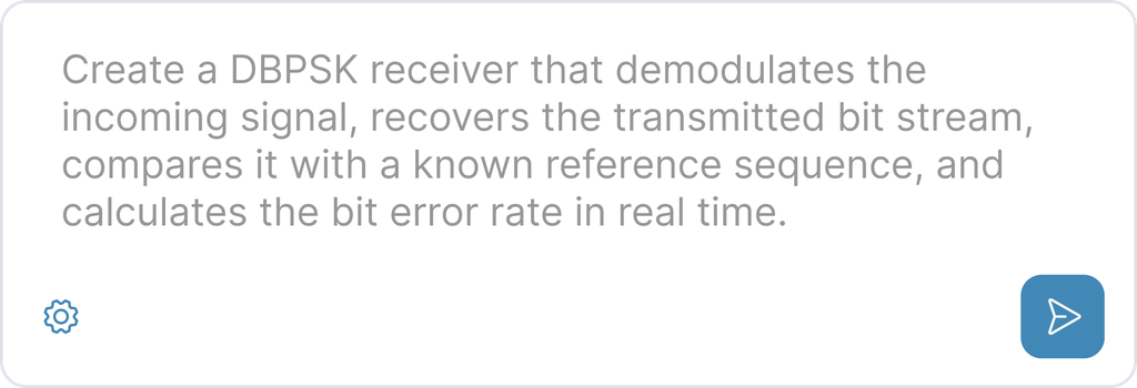
The conversation with GenInst Studio pushed the team to define each stage of the receiver more precisely: what signal needed to be processed, how bit decisions should be made, how the reference sequence should be used, and how the BER should be calculated. “This interaction helped turn a functional description of the receiver into specific requirements for the instrument,” said Torres Zafra.
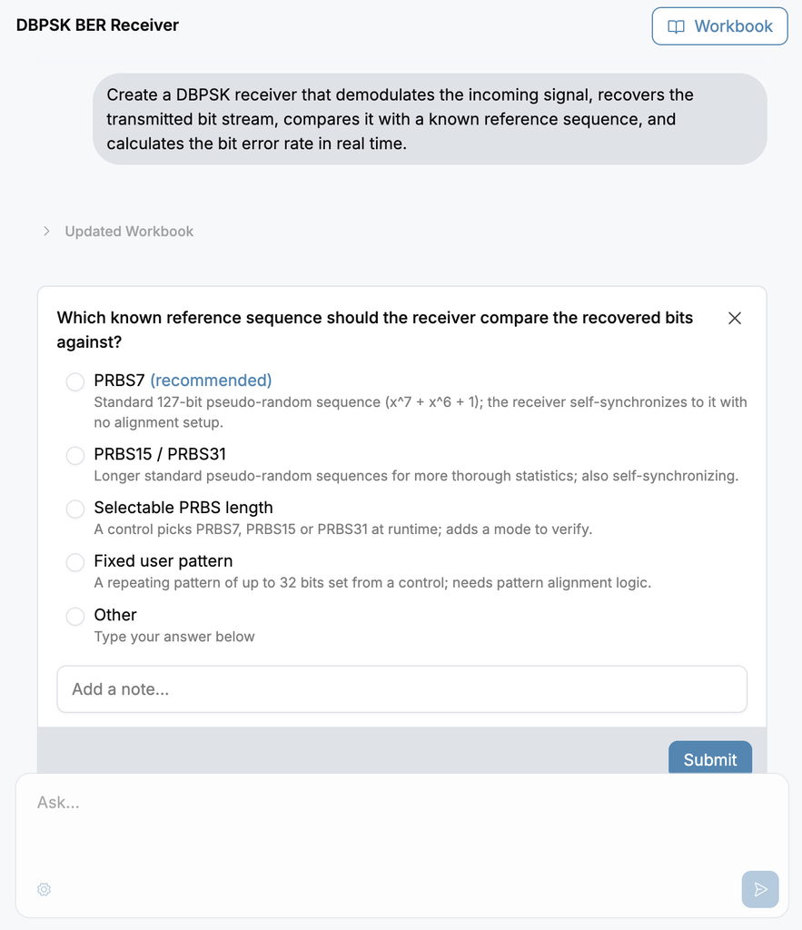
From there, the workflow followed four steps:
- 描述 the required functionality in natural language.
- 优化 the requirements together with GenInst Studio.
- Generate and validate the instrument using GenInst Studio’s built-in validation.
- 部署 the instrument to Moku and test it with experimental signals.
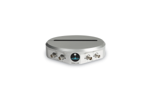
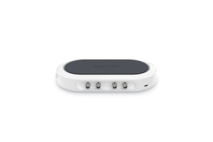
The result was a custom instrument implementing DBPSK reception, allowing the team to recover the demodulated data and measure BER directly on the hardware. The group regularly uses both Moku:Lab and Moku:Go in its experiments.
GenInst Studio’s validation process proved valuable before the instrument ever touched the optical setup. It allowed the team to check the instrument logic in advance and reduced the number of iterations a manual FPGA implementation would have required. Final confidence came from experimental testing. By using known signals, the team confirmed that the receiver correctly recovered the DBPSK data, enabled BER calculation, and behaved as expected.
结果
Using GenInst Studio, the GDAF team built a functional DBPSK receiver and used it to measure BER directly on Moku across a range of transmission rates in their optical communication experiments, obtaining BER values of around 3.5 × 10⁻³ in some configurations. The team is now preparing these results for publication in a scientific paper.
The first working version of the instrument was ready within a few days. An equivalent implementation through conventional FPGA development would have taken considerably longer once HDL design, simulation, integration, compilation, and debugging were accounted for.
Beyond saving time, GenInst Studio removed the need to build the FPGA logic from scratch in VHDL or Verilog, significantly lowering the barrier to creating specialized instrumentation. It also made an experiment practical that would otherwise have been difficult: an integrated DBPSK receiver with live BER measurement would not have been achievable with standard instruments alone, and would have demanded far more effort through FPGA development or external processing.
“The most valuable outcome was realizing that we could go from a very specific experimental need to a functional instrument in just a few days, without having to carry out a full FPGA development,” said Dr. Torres Zafra. “Having DBPSK reception and BER measurement directly available turned an experimental idea into a practical tool that we could actually use.”
The ability to describe a new function, adjust its requirements, and quickly generate a new version has also changed how fast the group can test ideas. Rather than starting from HDL design, development now starts from what the experiment needs, while the option of moving to a more specialized FPGA implementation later remains open.
展望未来
The team sees clear opportunities to apply GenInst Studio across its optical communications research, including new transmitters and receivers, PRBS sequence generation and detection, automated BER measurement, synchronization, filtering, and VLC channel characterization.
They are also interested in multisine signals and custom test sequences for the dynamic characterization of LEDs, photodetectors, and optical channels.
For other researchers with highly specific measurement needs, Dr. Torres Zafra recommends starting with a clear definition of the instrument’s inputs and outputs, the processing required, and how the result will be validated. “Tools such as GenInst Studio can help create a first functional instrument quickly, but it is still essential to experimentally verify its behavior using known signals and controlled conditions.”
As he puts it, one of GenInst Studio’s most important qualities is that it shortens the time between an experimental idea and a functional instrument. “For research groups that need highly specific instrumentation but do not necessarily have dedicated FPGA development resources, this approach can make it possible to explore experiments that would otherwise require much more time and effort.”
Make an account and try GenInst Studio for free.