


An introduction to I2C protocol
There are many ways of packaging and transmitting digital data. Whereas some protocols, such as UART, work well for point-to-point communications, they are not designed to handle a bus containing multiple devices. By contrast, protocols such as Inter-Integrated Circuit (I2C) are designed for synchronous, multi-device communication. A typical I2C bus contains at least one “master” device (although there can be more than one), and at least one “slave” device. Each slave device has an “address” that the master device can use to initiate communication. An I2C bus contains only two lines, the data line (SDA) and clock line (SCL), which are shared by all devices. This makes I2C an ideal protocol for connecting multiple sensors, clocks, or chips to a microcontroller, as the number of required lines does not increase with each device. Figure 1 shows a typical sequence captured by the Moku Logic Analyzer. Bit 0 carries the SDA line, and Bit 1 carries the SCL line. The first byte of the transmission contains the slaves address and initiates a read/write operation. If the address matches and slave acknowledges, the rest of the message is sent. In this case, the message is a series of four 8-bit digits.
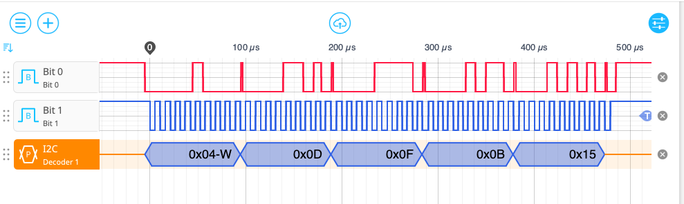
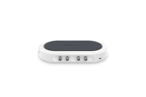
In this application note, we will use a Moku:Go as the master in an I2C protocol and make use of GenInst Studio to develop an instrument that can package and send I2C-encoded messages. We show how the open-drain architecture of Moku:Go allows its Logic Analyzer to listen to its own messages. Finally, we add an external microcontroller to act as the slave unit and confirm the data transmission.
Push-pull vs open-drain pins
I2C requires two digital lines, called SDA and SCL. SDA carries the digital data, and SCL carries a clock signal that lasts for the length of the message. As seen in Figure 1, the digital lines are held high when not transmitting and are pulled low during transmission.
In order to ensure proper and safe data transmission, it is essential that the architecture of the digital pins matches the requirements of the protocol. There are two types of pins supported on Moku:Go: push-pull and open-drain. Push-pull lines can drive to zero or high voltage, making them useful for fast, responsive data transfer in protocols like UART. However, since I2C devices share the bus, using push-pull pins can result in a short circuit if one pin is pulled high while another on the same bus is pulled low. By contrast, open-drain outputs only drive the lines low and rely on a pull-up resistor to be able to return to high (Vcc) voltage after a device releases the line.
Open-drain pins are required for I²C because they prevent short circuits when multiple devices share the same lines and enable the bidirectional communication necessary for the protocol to function. This configuration is seen in Figure 2, where the data lines are joined to Vcc by a pair of resistors. The value of the resistors should be chosen to gently guide the lines back to Vcc (either 3.3 V or 5 V depending on logic level). Too small a resistance exceeds the maximum sink current the devices and raises the low-level voltage, whereas too large a resistance slows the rising edges, since the rise time is set by the pull-up resistance and the bus capacitance.
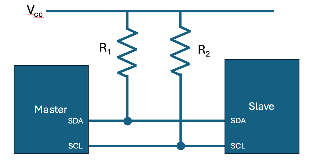
As of MokuOS 4.4.0, Moku:Go has the option to set its DIO ports as either input, output, or open-drain, allowing it to be used in a wide variety of protocol and logic analysis applications.
Creating an I2C Bus Master with GenInst Studio
In the next section we construct and test a I²C setup. In order to use the Moku Logic Analyzer to decode I2C sequences, we need to first create a Bus Master capable of packaging and encoding data bytes in an I2C format, such as those seen in Figure 1. The I²C bus master sends and receives data at configurable speeds, outputs the bus signals on selectable bits for use with the Moku:Go digital I/O, and reports transaction status and errors back to the user.
To do so, we make use of GenInst Studio, an AI-enabled development tool which takes plain language prompts and creates verified instruments, ready to deploy on Moku, complete with custom UIs. While the exact prompt used in GenInst Studio can vary substantially, the module should perform the following core functions:
- Generate complete I2C transactions (start, data bytes, acknowledge, stop) with correct bus timing
- Support both write and read transactions, plus repeated start conditions
- Send up to four data bytes to a target device at a user-specified 7-bit address
- Run at an adjustable clock speed from 1 kHz to 1 MHz
- Output the data and clock signals on user-selectable bits of a single 16-bit output, so they can be fed directly to the Moku:Go digital I/O pins
- Read back the target acknowledge/not-acknowledge responses (and received data) through the input
- Report status information, including whether a transaction is in progress, whether the target acknowledged, the last byte received, how many bytes were transferred, and any errors (such as lost arbitration or timeout)
After creating and verifying the model through GenInst Studio’s automated testbench, we are ready to deploy it on the Moku:Go. First, we construct the physical setup, with the following materials:
- Moku:Go device
- 16-bit breakout cable for Digital I/O (included with Moku:Go)
- Two 5.1 kΩ resistors
- Breadboard
We choose 5.1 kΩ for the standard I2C data rate (100 kHz). For higher data rates, reduce the resistance. We arrange the configuration as shown in Figure 3. Four leads (5 V, Pin 1, Pin 2, and Ground) are used. The 5 V lead is attached to the power rail of the breadboard and the Ground lead is attached to the grounding rail. Each Pin is connected to the voltage rail through a pull-up resistor.
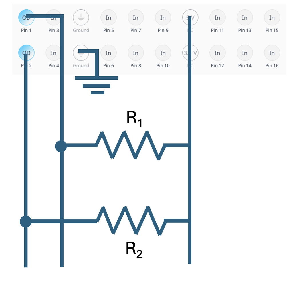
With the I2C Bus Master and physical connections in place, we can now send an encoded message and view it with the Moku Logic Analyzer.
Decoding I2C sequences with the Logic Analyzer
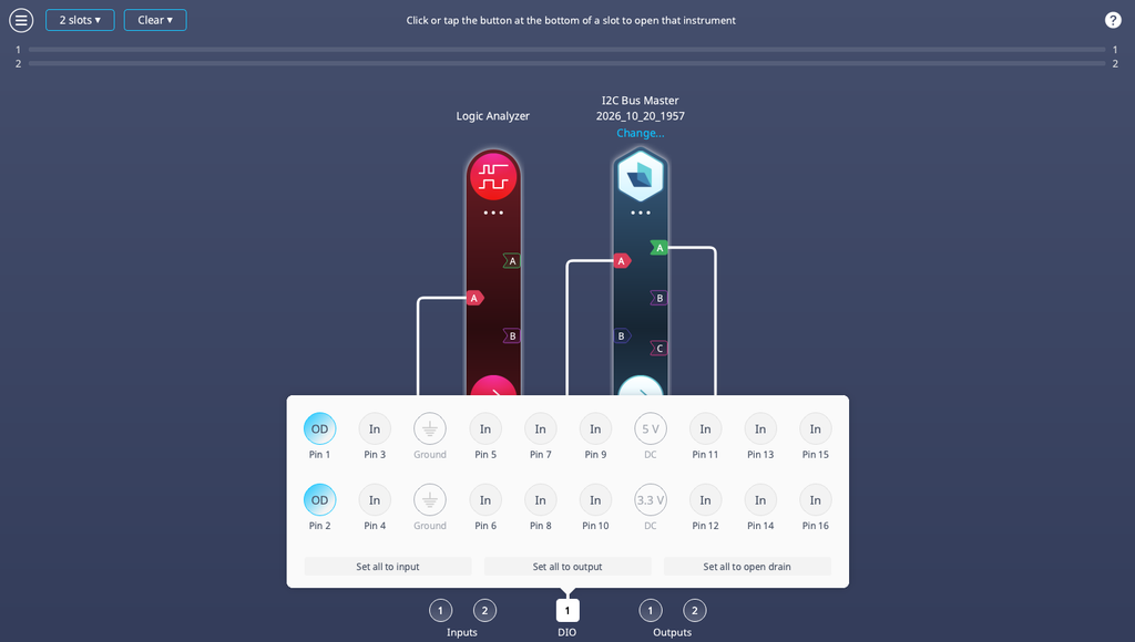
We now connect to our Moku:Go and launch the Moku Logic Analyzer alongside the Bus Master to decode the protocols. From the instrument select screen, we choose Multi-Instrument Mode. We place the Logic Analyzer in Slot 1 and GenInst-created I2C Bus Master instrument in Slot 2, as seen in Figure 4. Internally, we connect the Bus Master output, Bus Master input, and Logic Analyzer input all to the DIO channel.
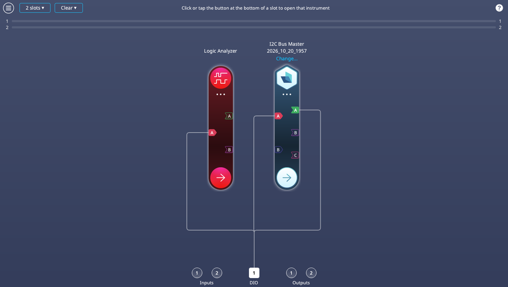
On the screen, click the box above DIO to open the configuration screen. You can click on the circle corresponding to each pin to rotate between output, input, and open-drain. Set Pin 1 and Pin 2 to open-drain – the remainder of the pins are not used in this example. See Figure 5 for details. Once you have set the instruments, pins, and connections, click Apply in the top right.
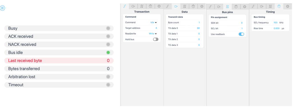
First we configure the Bus Master to output a single 8-bit (0-255) number encoded in I2C format. We click the arrow on the I2C Bus Master instrument to open the configuration screen.
Note: the following UI was created alongside the instrument using GenInst Studio. The exact format, layout, and nature of the interface can vary depending on your exact prompt and/or requirements.
Opening the custom UI, we first click over to the Transaction tab. We set “Command” to Idle for now, but we will use this option to send the message later. We set the “Target address” to 4, and “Read/write” to Write. On the Data tab, we set the Byte count to 1 and Tx data 0 to “60.” You can choose any arbitrary number between the values of 0 and 255 for the data value. On the Bus pins tab, we set the SDA bit to 0 and the SCL bit to 1. These values determine what pins of the DIO we use for the data lines. We also enable the “use readback setting” so the Bus Master can receive the ACK/NACK from the slave device.
Note: Indexing on the Moku:Go DIO pins begins at 1. Indexing of the bit handling within the Moku instruments begins at zero. In this case, Bit 0 is carried on Pin 1 and Bit 1 is carried on Pin 2.
Finally, on the Timing tab, we set the SCL frequency to 100 kHz, which corresponds to the standard mode data transfer rate. All of these settings can be seen in Figure 6.
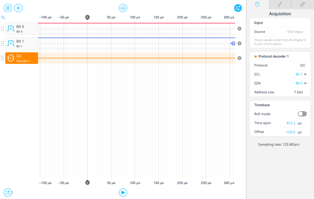
Moving over to the Logic Analyzer instrument, we monitor only Bits 0 and 1, which carry the SDA and SCL lines, respectively. We click the plus sign and add an I2C protocol decoder, which will appear below the traces for the two bits. On the Acquisition tab, we set the correct bits for SCL and SDA, as seen in Figure 7. Before switching back to the Bus Master, ensure that the traces on Bit 0 and Bit 1 remain at high voltage – this is the default state when there is no data transfer. If the channels are not high, there may be an issue with the connections or pull-up resistors.
Lastly, on the Trigger tab, set the Mode to Normal, Channel to Bit 1, and the Edge to Falling. This will ensure that the Logic Analyzer captures a single data transfer sequence for analysis.
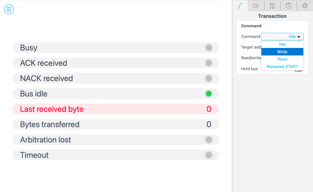
Moving back over to the Bus Master, we first confirm that the “Bus idle” light is lit, as seen in Figure 8. We move to the Transaction tab and select Write from the drop-down menu to send a single trace. In the other window, the Logic Analyzer will acquire a trace.
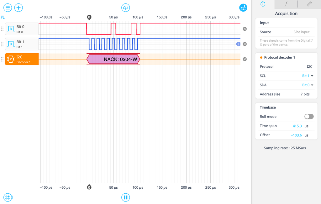
Note that the “NACK received” light is now lit. This is because there is no device with the address of 4 on the bus line, so no slave device acknowledges the message. The Logic Analyzer is totally passive and cannot act as a receiver – it is only for listening to data transfer between the master and slave device. We can confirm this by looking at the trace acquired by the Logic Analyzer. We see the SDA and SCL data captured, as well as the decoded message: NACK: 0x04-W, meaning a message was sent to address 4 and not acknowledged.
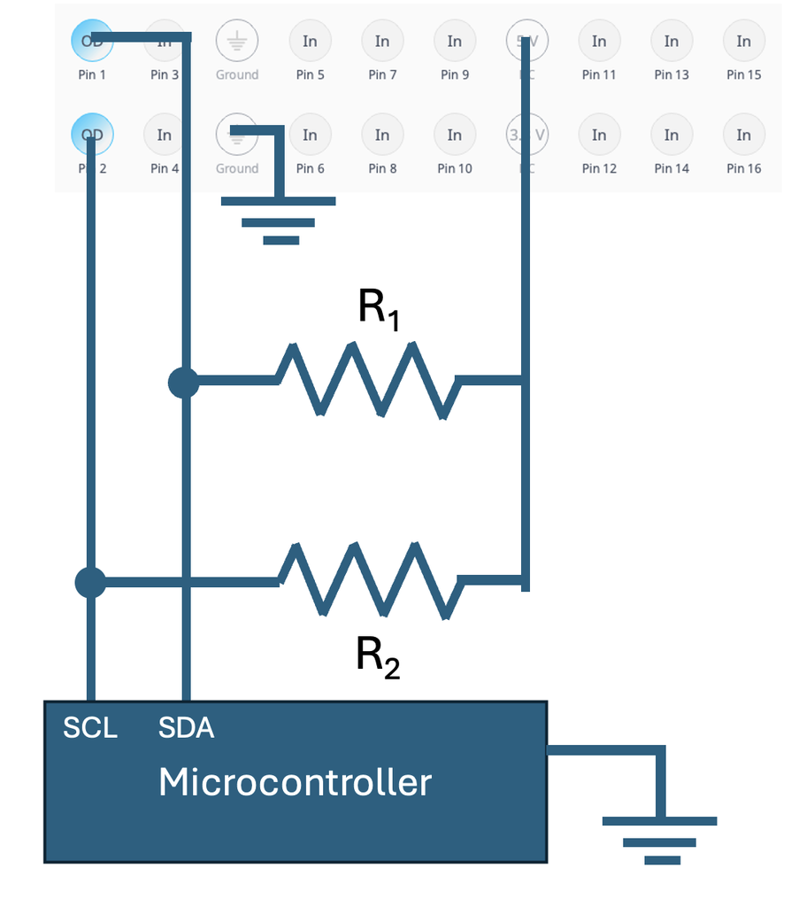
To test the full sequence, we add a microcontroller unit (MCU) to the line, connecting its SDA and SCL to the breadboard so that they are joined to the respective lines from the Moku DIO. The MCU used in this case is an Arduini Uno R3. The MCU has dedicated SDA and SCL ports, and its internal logic is fully compatible with I2C protocol using 5 V TTL logic. The MCU does have “weak” (high resistance) internal pull-up resistors which can be supplemented by the external pull-up resistors to achieve higher transfer speed. The MCU also can be assigned a 7-bit address using a short script. The full configuration can be seen in Figure 10.
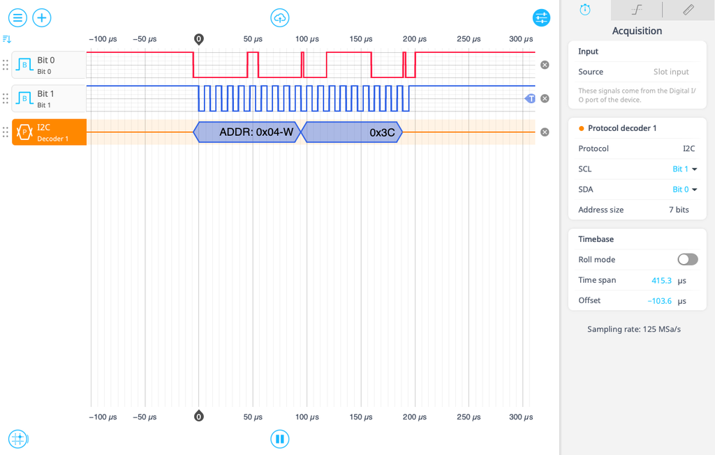
With the slave device in place, we return to the Bus Master interface and confirm that the bus is idle and ready to send again. We click “Write” from the drop-down menu to resend the sequence. This time, the “ACK received” light should show. We confirm this successful send of the data by going once more to the Logic Analyzer and looking at the latest trace capture, which is seen in Figure 11. The sequence should be longer (since both the address and the message are sent in this instance), and the I2C protocol decoder should display both the correct address (4) and the correct data byte. Note that the Logic Analyzer will display the number 60 in hexadecimal as 3C, but regardless this confirms that the data has successfully transferred from the Moku master device to the MCU slave device.
Summary
In this app note, we have shown how the Moku’s flexible DIO pins, ready-to-deploy Logic Analyzer, and custom instrumentation through GenInst Studio make it a versatile option for I2C applications. The DIO pins support both push-pull and open-drain configurations, enabling its use in both multi-device and point-to-point digital communications. The Logic Analyzer features decoders for a wide variety of digital protocols, including I2C. Finally, GenInst Studio allows users to implement custom functions and instrumentation directly on the Moku FPGA without the need to code, debug, or validate HDL code themselves. This allows Moku:Go to serve effectively as transmitter, receiver, or decoder for an enormous array of digital communication protocols.