Introduction
As discussed in the previous control theory application note series, frequency domain analysis plays a critical role in designing and evaluating feedback systems, particularly in assessing their stability and overall noise rejection performance. While earlier notes focused on theoretical principles in the Laplace domain, this application note shifts to the practical implementation of those concepts using a real-world example involving Moku:Pro and a voltage-controlled oscillator (VCO), which is an electronic oscillator whose output frequency varies in response to an applied control voltage, allowing precise frequency tuning and modulation for applications such as signal generation and communication systems.
A phase-locked loop (PLL) is a feedback system that aligns the phase and frequency of an output signal with a reference input. It does so by continuously adjusting the VCO output frequency based on the phase difference between the reference and the feedback signal, as detected by a phase detector. PLLs are widely used in communication systems, signal synthesis, and clock recovery due to their ability to produce stable, low-jitter signals and accurately track varying reference frequencies. They also form the core of the Moku Phasemeter, which is known for high precision phase and frequency measurements without dead time or phase wraps.
This application note describes the construction of a phase locked loop (PLL) using the Moku Lock-in Amplifier, along with the measurement and optimization of its open-loop transfer function (OLTF). The process begins with an initial controller configuration determined through empirical tuning. The OLTF is first modeled and then validated with experimental measurements to assess key stability metrics, including phase- and gain- margin. These results inform an optimization process aimed at increasing low-frequency gain while preserving sufficient stability margins. Finally, frequency noise measurements from both the initial and optimized controllers are compared to evaluate the improvement in feedback loop performance.
Experimental Setup
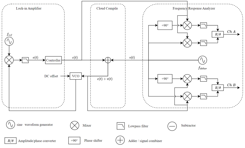
Stabilizing a VCO requires a frequency reference, typically provided by a highly accurate source such as a rubidium-disciplined clock. In this experiment, the reference is supplied by the Moku Pro’s high-precision internal waveform generator, which functions as the local oscillator within the Lock-in Amplifier module.
Moku platforms offer two primary methods for extracting the phase difference—also referred to as the error signal—used in the feedback control of the VCO. The first method employs the Phasemeter to directly track the frequency and phase of the VCO output. The second method, employed in this application, utilizes the Lock-in Amplifier to demodulate the VCO signal with the local oscillator to produce the error signal. This approach is chosen for its structural simplicity and the convenience of the integrated proportional–integral–derivative (PID) controller, which generates the VCO control signal directly from the demodulated output.
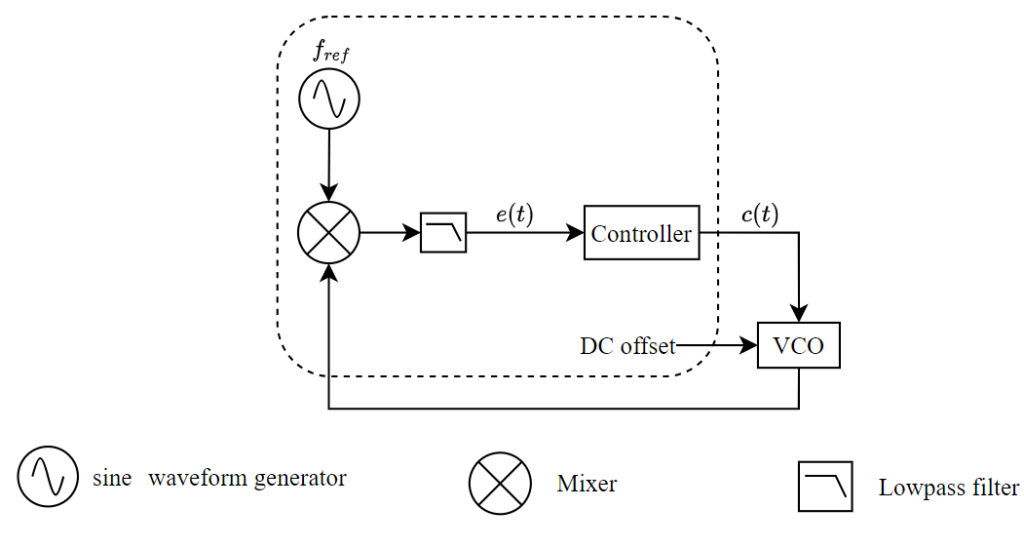
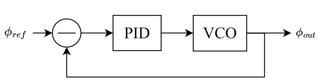
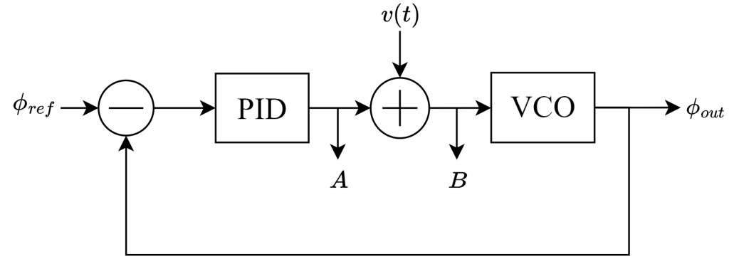
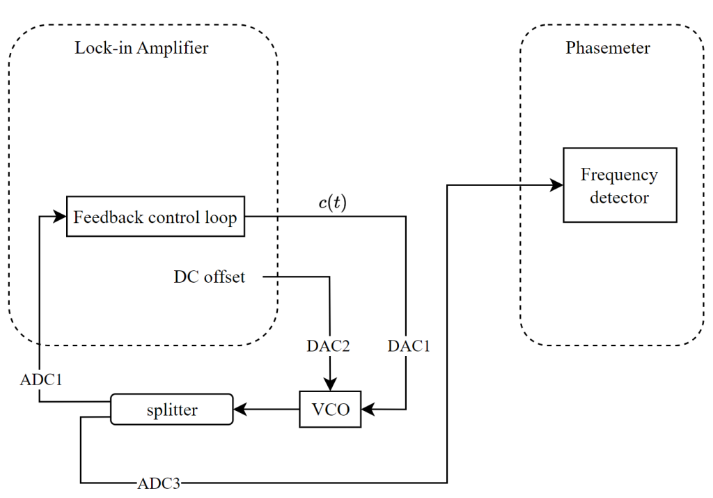
The block diagram of the PLL based on the Lock-in Amplifier is shown in Figure 1. It includes a reference sine wave generator \(f_{ref}\) (the local oscillator), a mixer for demodulation, a lowpass filter that removes the frequency sum component and produces the error signal \(e(t)\) , and a controller that generates the feedback control signal \(c(t)\) applied to the VCO’s tuning port to maintain frequency stability. Additionally, a DC offset is supplied to power the VCO.
Phase detector
For clarity and simplicity, this application note focuses on analyzing the system under locked condition. Under this condition, the error signal \(e(t)\), as depicted in Figure 1, represents the residual phase difference between the reference signal and the VCO output. This phase difference arises from the time-integrated frequency deviation between the two signals. By maintaining the phase error at or near zero, the system ensures that the VCO output frequency remains locked to the reference. The error signal \(e(t)\) is mathematically expressed as:
\(e(t) = A \sin{\left( \int f_{VCO}(t)dt \right)} \times \sin{ \left( \int f_{ref}dt \right) } = \frac{A}{2} \cos{\left( \int \left[f_{ref} – f_{VCO}(t) \right] dt \right)} + \frac{A}{2} \cos{\left( \int \left[f_{ref} + f_{VCO}(t) \right] dt \right)}\).
The VCO nominal frequency in this setup is 62 MHz, while the lowpass filter has a cutoff frequency of 12.3 MHz, as will be shown in later sections. As a result, the additive frequency component is filtered out by the lowpass filter, leaving only the subtractive frequency component. Therefore, the error signal can be expressed as follows:
\(e(t) = \frac{A}{2} \cos{\left( \int \left[f_{ref} – f_{VCO}(t) \right] dt \right)} = \frac{A}{2} \sin{\left( \int \left[f_{ref} – f_{VCO}(t) \right] dt + 90^{\Large\circ} \right)}\)
In the locked state, where \(\phi(t) \approx -90^{\Large\circ}\), the error signal \(e(t)\) fluctuates only slightly around zero, primarily due to residual noise. Using Taylor’s expansion, a sine waveform can be expressed as
\(\sin{x} = x-\frac{x^3}{3!} + \frac{x^5}{5!}-\frac{x^7}{7!} + …\)
When \(x\) oscillates only slightly around zero in the locked state, the sine waveform exhibits good linearity at this point because higher-order components are negligible. This allows the approximation \(sin{x} \approx x\). Therefore, the amplitude of \(e(t)\) provides a direct indication of the phase error, albeit with a constant 90° phase offset present between the local oscillator and the VCO output.
Furthermore, the gain of the phase detector is amplitude-dependent and varies with the magnitude of the VCO signal. This dependence must be considered when evaluating the performance of the control system. As a result, the error signal can be approximated by the expression:
\(e(t) \approx \frac{A}{2} \times \left( \phi(t) + 90^{\Large\circ} \right) \)
Where \(A\) represents the amplitude of the VCO signal and \(\phi(t) \) denotes the instantaneous phase deviation.
Lock-in Amplifier configuration
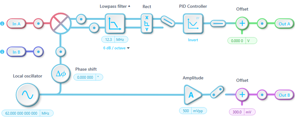
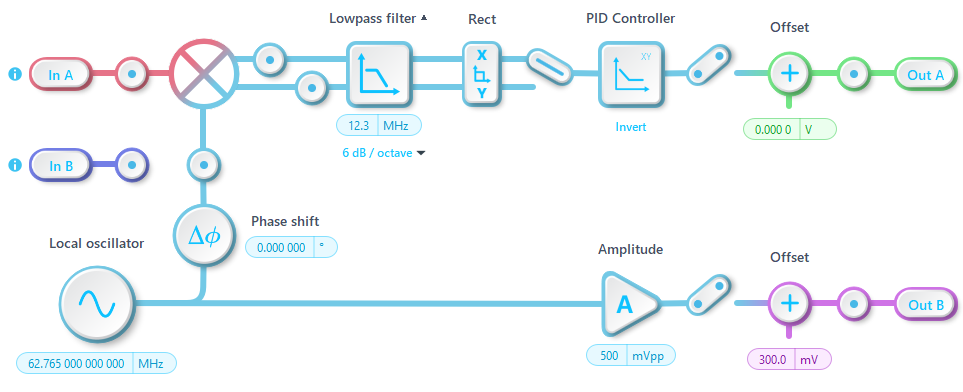
Following the PLL block diagram shown in Figure 1, the Lock-in Amplifier configuration is illustrated in Figure 2. The VCO output signal is fed into InA, while the local oscillator is set to the nominal VCO frequency of 62 MHz. The lowpass filter cutoff frequency is set to its maximum value of 12.3 MHz. This setting effectively suppresses the frequency sum component and maximizes the control bandwidth by reducing phase delay introduced by the filter within the feedback loop. The control signal for tuning the VCO frequency is output through OutA, and OutB provides a steady 300 mV DC voltage to power the VCO.
Notably, the error signal \(e(t)\) is assigned to the X channel, which uses the in-phase component as the error signal. Because of this, the locked VCO output exhibits a 90° phase difference relative to the local oscillator. This phase offset could be removed by routing the error signal to the Y channel, which uses the quadrature component instead. However, for the purposes of this application note, the phase offset is acceptable, so the PLL continues to use the X channel output as the error signal.
Initial lock using a PI controller
The experimental Multi-Instrument Mode setup is shown in Figure 3. Here, the Phasemeter assigned to Slot 4 continuously monitors the VCO frequency. This measurement provides an accurate estimate of the VCO’s initial frequency, allowing the local oscillator frequency in the Lock-in Amplifier to be set appropriately. This method is commonly referred to as assisted frequency acquisition. As an alternative, the Moku Spectrum Analyzer may also be used to identify the VCO output frequency by locating its spectral peak.
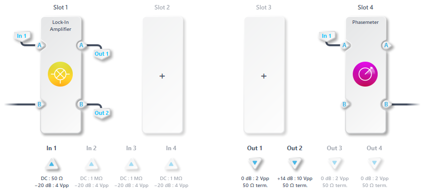
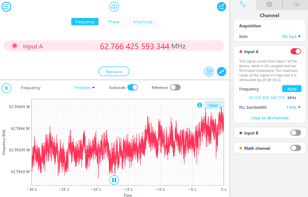
The free-running VCO frequency is measured using the Phasemeter, with the frequency setting in Auto mode. The automatically acquired initial frequency is 62.7654 MHz. The internal reference frequency of the Lock-in Amplifier is adjusted to match the initial frequency of the VCO to facilitate reliable initial locking. Based on this measurement, the local oscillator is set to 62.765 MHz, as shown in Figure 5.
For initial locking, a proportional–integral (PI) controller is configured using a rough estimate and empirical experience to enable the feedback loop to function. At this stage, the PI controller is not optimized, especially considering that the loop contains two pure integrators: one from the PI controller itself and the other from the VCO’s frequency-to-phase relationship. This configuration introduces a cumulative 180-degree phase shift within the loop, which can predispose the system to closed-loop instability.
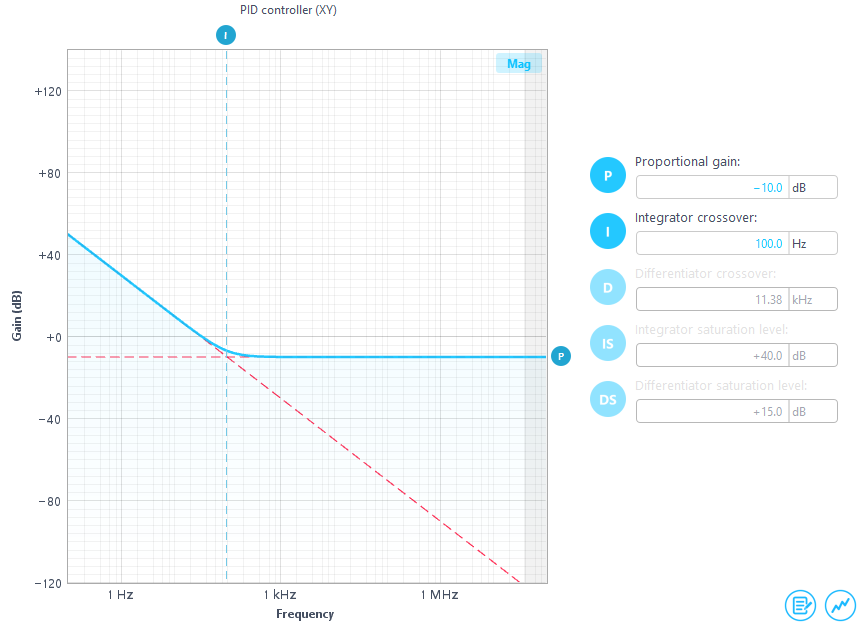
The PI controller parameters are displayed in Figure 6. The proportional gain is set to –10 dB, and the integrator crossover frequency is configured at 100 Hz. As a result, the controller operates with limited bandwidth. It responds slowly to phase deviations and provides only modest open-loop gain, offering limited suppression of VCO frequency noise.
After engaging the PI controller, the measured frequency from the Phasemeter is shown in Figure 7. Before locking, the signal exhibits a constant frequency offset and large frequency variations. Once the PI controller is active, the frequency locks to 62.765 MHz, with fluctuations negligible at the chosen vertical scale. This demonstrates the effectiveness of the closed-loop feedback stabilization.
The remaining frequency noise of the VCO is measured using the Phasemeter, which continuously logs the frequency data as shown in Figure 8. The VCO locked with the PI controller shows reduced frequency variations in the time domain compared to the free-running VCO. The peak-to-peak frequency noise decreases from ± 800 Hz in the free-running case to ± 100 Hz after locking.
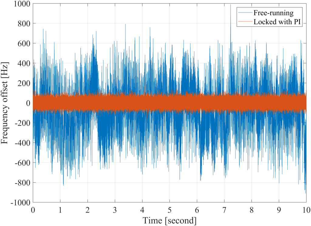
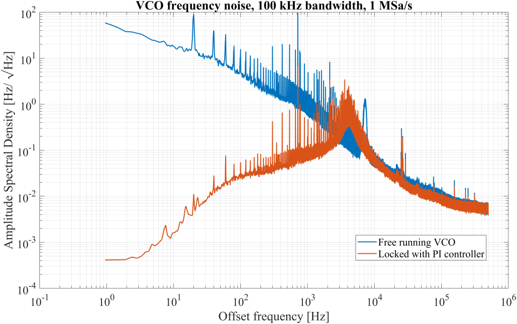
Figure 9 presents the amplitude spectral density (ASD) of the frequency noise for both the free-running and PI-locked VCO. In the free-running case, small spectral tones are observed at 20 Hz and its harmonics, likely originating from subharmonic interference related to the power grid.
A distinct noise peak appears near a 4 kHz offset frequency in the PI-locked ASD. Ideally, the control loop should suppress phase and frequency noise across the bandwidth without introducing additional noise components.
The presence of this peak suggests that the phase margin of the loop may be insufficient. When the phase margin is too small, the loop gain and phase response can produce a resonant behavior near the unity-gain crossover frequency, amplifying noise instead of attenuating it. This effect, known as noise peaking, indicates that the loop dynamics may need adjustment. The issue is examined further in the OLTF analysis in the next section, and a similar topic is also discussed elsewhere in this application note.
Open-loop transfer function measurement
Optimizing the stability and performance of the VCO feedback system requires a detailed understanding of its frequency-domain behavior. The OLTF is a critical tool in this analysis, as it provides insights into system gain, phase margin, and overall stability. These characteristics directly inform how the proportional, integral, and derivative components of the controller should be adjusted. This section begins by introducing the OLTF and the method used to obtain it, followed by a discussion on how it guides system optimization.
Loop model
A simplified model of the feedback loop is shown in Figure 10. In this model, the phase detector is represented as a subtractor, reflecting its function in the locked condition: it outputs the phase difference between the reference signal and the VCO output. As previously described, the demodulation process is responsible for generating this phase error. Under locked conditions, the error signal takes the form:
\(e(t) = \phi_{ref} – \phi_{out} \)
which serves as the input to the controller. With this foundation, the OLTF can be derived and measured to evaluate system stability and guide parameter tuning in a systematic way.
The feedback loop in the Laplace domain can be modeled by the following equation, where \(\text{PID}(s)\) and \(\text{VCO}(s)\) represent the transfer function of the PID controller and the VCO, respectively. Note that the phase detector (subtractor) is assumed to have unity gain for simplicity. In experiments, recognition and compensation for the phase detector gain will be necessary during system modeling.
\(\left(\phi_{ref} – \phi_{out}\right) = \text{PID}(s) \times \text{VCO}(s) = \phi_{out}\)
Rearranging the loop, the closed-loop transfer function (CLTF) \(H(s)\) is given by:
\(H(s) = \frac{\phi_{out}}{\phi_{ref}} = \frac{\text{PID}(s) \times \text{VCO}(s)}{1 + \text{PID}(s) \times \text{VCO}(s)} = \frac{G(s)}{1+G(s)}\)
Where \(G(s) = \text{PID}(s) \times \text{VCO}(s)\) is the OLTF. \(G(s)\) plays a central role in determining the behavior of the closed-loop system. Since \(G(s)\) appears in both the numerator and denominator of the closed-loop transfer function \(H(s)\), its properties directly influence system stability. Of particular importance is the condition where \(G(s)=-1\), which causes the denominator of \(H(s)\) to approach zero—leading to unbounded gain and instability. This critical point must be carefully avoided in feedback system design.
To assess how close the system is to this instability threshold, frequency-domain stability metrics such as gain margin and phase margin are used. This section focuses on evaluating these margins to determine the robustness of the control loop and to guide further tuning of controller parameters.
The initial step in OLTF \(G(s)\) characterization is to determine the transfer function of the VCO. This is achieved by injecting a swept-frequency dithering signal into the VCO’s tuning port and analyzing the corresponding frequency change of the VCO output.
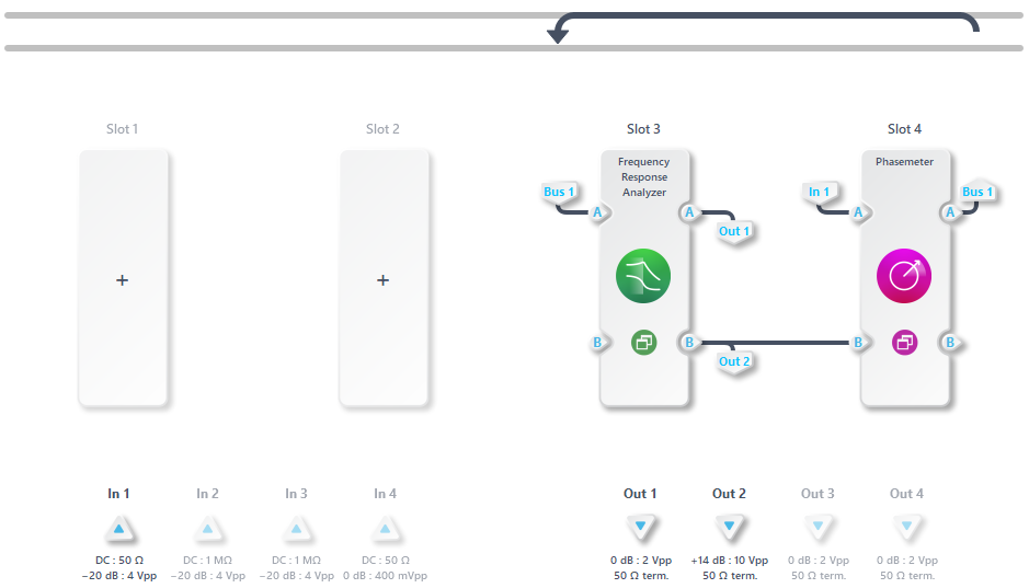
Figure 11 illustrates the setup used to characterize the transfer function of the VCO. In this configuration, the Frequency Response Analyzer generates a low-amplitude swept-frequency dithering signal, which is output through OutA and applied to the frequency tuning port of the VCO. While this signal stimulates the VCO, the Frequency Response Analyzer simultaneously performs magnitude and phase response measurements.
The instantaneous output frequency of the VCO is measured by the Phasemeter, converted into a voltage signal using a frequency-to-voltage scaling factor of 10 µV/Hz, and then fed back into the Frequency Response Analyzer. This arrangement enables automated and accurate determination of the VCO’s transfer function.
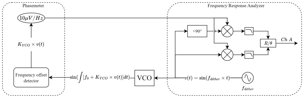
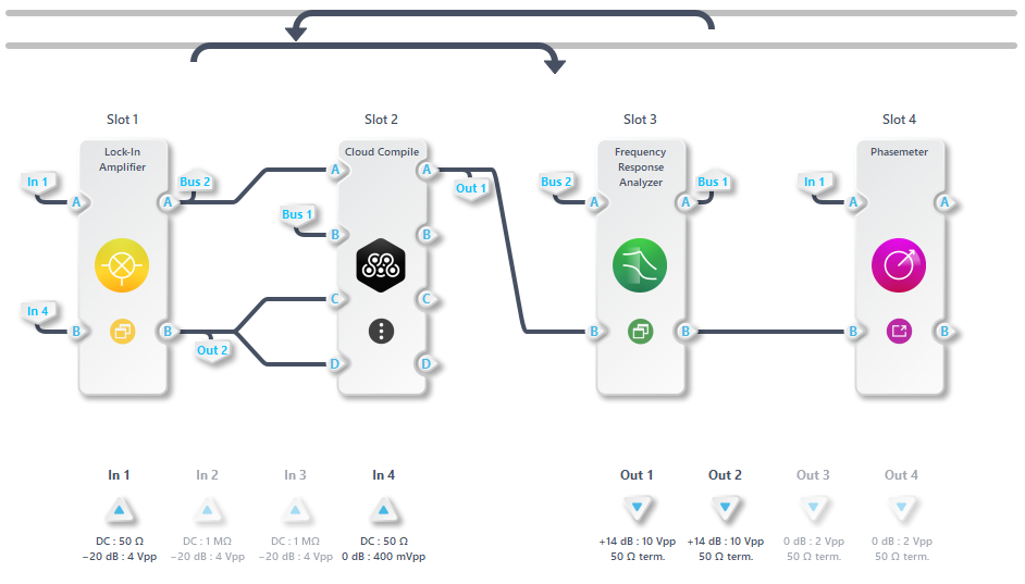
Figure 12 shows the Moku:Pro Multi-Instrument Mode configuration used for transfer function measurement. The output of the VCO is connected to InA of the Phasemeter, which continuously monitors the VCO’s frequency. This frequency data is then transmitted via an internal signal bus to InA of the Frequency Response Analyzer.
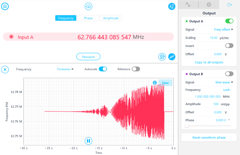
The Phasemeter user interface is shown in Figure 13, displaying the measured time-domain frequency trace. The frequency offset is sent to the Frequency Response Analyzer for transfer function measurement. From the displayed data, it is evident that the VCO frequency deviation increases over time. It is important to note that the Frequency Response Analyzer dithering output amplitude remains constant while sweeping the dithering signal frequency. It indicates that the VCO can only follow the dithering signal effectively when the dithering signal is varying slowly. Hence, it can be modeled as a lowpass response.
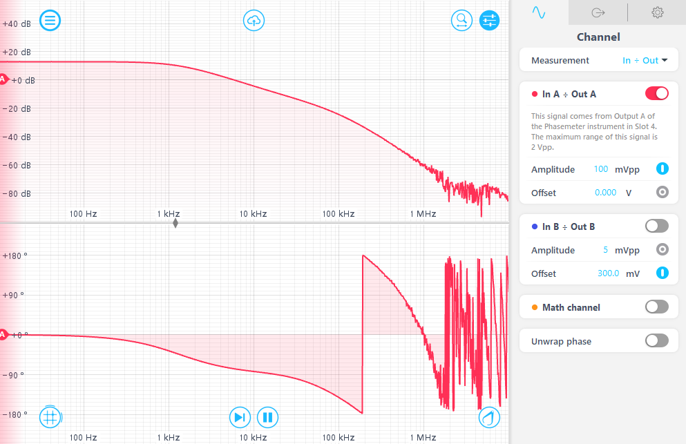
The frequency offset is then processed by the Frequency Response Analyzer, which measures the magnitude and phase of the signal across a range of dithering frequencies. The measured response of the VCO is shown in Figure 14. The lowpass corner frequency is estimated at 9.538 kHz, and the VCO gain is approximately 83,497 Hz/V.
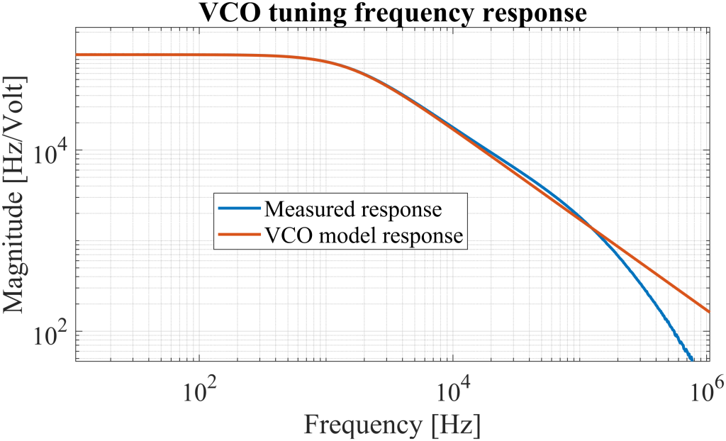
The VCO frequency response, presented in Figure 15, is derived by normalizing the measured frequency response using the Frequency Response Analyzer with the Phasemeter’s frequency-to-voltage conversion factor. While the response appears to exhibit two poles, the second pole arises from the limited tracking bandwidth of the Phasemeter and can therefore be neglected. By combining the VCO response with that of the controller, the OLTF can be determined. The lowpass filter within the Lock-in Amplifier is excluded from this analysis, as its corner frequency of 12.3 MHz lies well beyond the frequency range of interest and has no significant influence on the OLTF in the low-frequency regime.
To model the system in MATLAB, the OLTF can be constructed as follows. The PI controller model is based on the s domain representation described in the previous control series application notes.
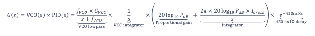
The system parameters are configured as follows: \(f_{VCO} = \text{9.538 kHz}\), \(G_{VCO} = \text{83,497 Hz/volt}\), \(P_{dB} = \text{-10 dB}\), and \(I_{cross} = \text{100 Hz}\). It is important to note that the OLTF includes a VCO integrator, representing the frequency-to-phase conversion, since the detected error signal in the Lock-in Amplifier is expressed in phase. Additionally, the 450 ns delay accounts for the Lock-in Amplifier processing delay and input-to-output latency in the Moku:Pro. Once the model is established, the next step involves measuring the actual OLTF and comparing it with the modeled response to validate its accuracy.
Loop measurement
Referring to the previously released application note in the control theory series, the block diagram for measuring \(G(s)\) is shown in Figure 16. In this setup, the dithering signal is injected at the point between the PID controller and the VCO.
The transfer functions at points A and B within the feedback loop can be derived from the system’s response to an externally injected dithering signal. During this measurement, the reference phase \(\phi_{ref}\) is set to zero, meaning the phase detector contributes only a negative sign to the loop.
At point A, the transfer function can be expressed as:
\(\left( A(s) + V(s) \right) \times \text{VCO}(s) \times -1 \times \text{PID}(s) = A(s)\)
where \(V(s)\) is the Laplace transform of the injected dithering signal \(v(t)\)
Rearranging this expression yields the transfer function from the injected signal to the output at point A:
\(\frac{A(s)}{V(s)} = \frac{-1 \times \text{VCO}(s) \times \text{PID}(s)}{1 + \text{VCO}(s) \times \text{PID}(s)} = \frac{-G(s)}{1+G(s)}\)
This expression shows that, under high loop gain \(G(s) \gg 1\), the output at point A closely tracks the negative of the input, i.e., \(\frac{A(s)}{V(s)} \approx -1\), which corresponds to negative reference tracking.
At point B, the relationship can be written as:
\(B(s) \times \text{VCO}(s) \times -1 \times \text{PID}(s) + V(s) = B(s)\)
Solving for the transfer function yields:
\(\frac{B(s)}{V(s)} = \frac{1}{1 + \text{VCO}(s) \times \text{PID}(s)} = \frac{1}{1+G(s)}\)
This indicates that, when \(G(s)\) is large, the signal at point B is significantly attenuated. Consequently, the transfer function at point B characterizes disturbance rejection, effectively suppressing the dithering signal \(V(s)\) at that point.
By taking the ratio of the transfer functions at points A and B, the OLTF \(G(s)\) can be recovered:
\(\frac{A(s)}{B(s)} = -G(s)\)
The experimental setup, illustrated in Figure 17, implements this concept. The dithering signal \(v(t)\) is injected into the VCO feedback loop via a Moku Cloud Compile configured as a simple adder. Both the control signal \(c(t)\) before injection and the combined signal \(c(t)+v(t)\) after injection are simultaneously measured using two channels of the Frequency Response Analyzer. This allows the system to capture the transfer functions at points A and B for analysis.
The Multi-Instrument Mode configuration is presented in Figure 18 and corresponds to the block diagram illustrated in Figure 17. It is important to note that the Phasemeter in Slot 4 is used solely for monitoring purposes and does not participate in the feedback control loop.
The Frequency Response Analyzer user interface is shown in Figure 19. In this setup, Channel A (red trace) represents the transfer function from the dithering signal \(v(t)\) to the control signal \(c(t)\). Channel B (blue trace) shows the combined signal \(c(t)+v(t)\), which represents the tuning input to the VCO. The OLTF is obtained by dividing the magnitude and subtracting the phase of Channel A from those of Channel B. The resulting OLTF is displayed on the Math channel (orange trace).
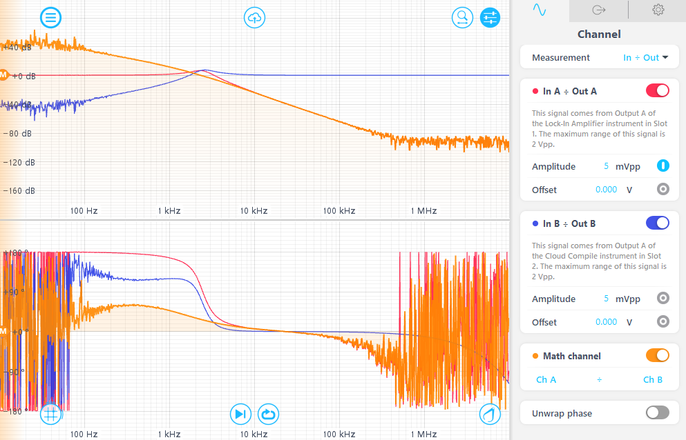
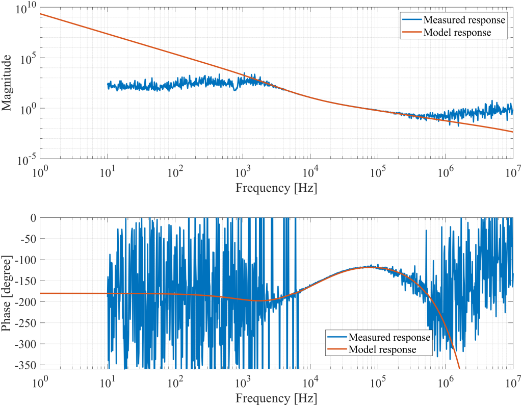
The OLTF model developed in the previous section is simulated in MATLAB and compared against the measured response obtained from the Frequency Response Analyzer, as shown in Figure 20. The simulation exhibits strong agreement with the measured data in both magnitude and phase. An additional 180° is subtracted from the measured phase response to account for the inherent phase inversion introduced by the negative feedback configuration.
The measurement is most accurate in the vicinity of the unity gain frequency. At higher frequencies, the control loop lacks sufficient bandwidth to track the injected dithering signal at point A (Figure 16), leading to reduced measurement fidelity. At the other end of the spectrum, very low frequencies are strongly suppressed by the loop, leaving only a minimal residual of the dithering signal \(v(t)\) at point B (Figure 16), which limits the usefulness of measurements in both low- and high-frequency regions.
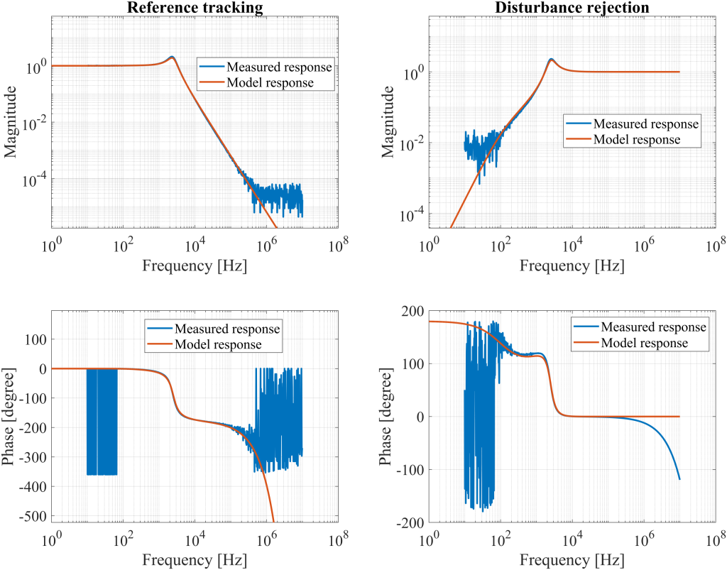
In addition to the OLTF shown in Figure 20, the reference tracking and disturbance rejection responses are also generated and displayed in Figure 21. In the measured reference tracking, the phase response is shifted by 180° because the measured response is \(\frac{-G(s)}{1+G(s)}\), rather than the typical \(\frac{G(s)}{1+G(s)}\) form.
A gain peak appears in the disturbance rejection response around 3 kHz, which corresponds to the noise peak observed in the measured frequency noise after locking shown in Figure 9. This gain peaking results from the small phase margin of the current OLTF, causing noise to increase rather than decrease.
Loop optimization
The primary motivation for measuring the OLTF and modeling the system is to optimize the performance of the locking loop. As discussed in the previous application note, the key indicators derived from the OLTF—loop gain, phase margin, and gain margin—are critical for evaluating and improving feedback system. An effective control system should maximize low frequency gain to suppress disturbances while maintaining sufficient phase and gain margins to ensure stability and robustness against noise and parameter variations.
Add 1 kHz differentiator term
As shown in the OLTF plot in Figure 20, the PI-controlled feedback loop features three contributing poles near the unity gain frequency. These arise from the VCO’s intrinsic integrator, which performs frequency-to-phase conversion, its 1st-order lowpass response, and the integrator component of the PI controller. Together, these three poles contribute a total phase shift of 270°, which poses a risk of instability if not properly managed.
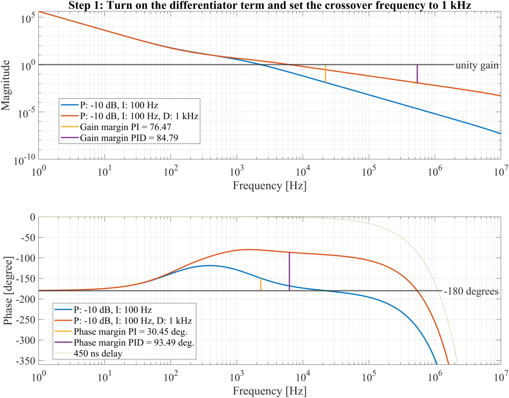
The unity gain frequency is situated between the 100 Hz crossover point of the PI integrator and the 9.538 kHz corner frequency of the VCO’s lowpass filter. In this intermediate region, the effect of the PI integrator is diminishing, whereas the lowpass pole’s influence is not yet fully established. This overlap produces a modest phase bump, placing the unity gain frequency in a zone that provides a limited but sufficient phase margin. As a result, the system maintains a phase margin of approximately 30° and a gain margin around 76.47, ensuring stable operation.
Figure 22 includes a reference line representing the 450 ns delay introduced by the Lock-in Amplifier’s processing time and the input-to-output latency. This delay does not yet limit the system’s phase margin, indicating room for additional phase compensation. To enhance stability, within the 1 to 100 kHz frequency range, a differentiator term can be added to the controller to provide up to 90° of phase lead. In this case, a differentiator with a crossover frequency of 1 kHz is introduced. The revised PID controller and its corresponding OLTF are expressed by the following equation:

The updated OLTF \(G_{PID}(s)\), which includes the differentiator term, is plotted in Figure 22 for comparison. The differentiator crossover frequency \(D_{cross}\) is set to 1 kHz, while all other parameters remain the same as in the previous PI-controlled loop \(G_{PI}(s)\). In Figure 22, the blue curve represents \(G_{PI}(s)\), and the orange curve represents the enhanced \(G_{PID}(s)\). The gain and phase margins for both configurations are also indicated. While the gain margins remain largely unchanged, the phase margin increases significantly—from 30.45° in the PI case to 93.49° with the PID configuration. This confirms the effectiveness of introducing the 1 kHz differentiator. Additionally, the unity gain frequency shifts higher in the PID case, indicating an increased control bandwidth.
Further optimization will focus on improving the magnitude response, as the phase response of the \(G_{PID}(s)\) is constrained by the inherent delay at higher frequencies.
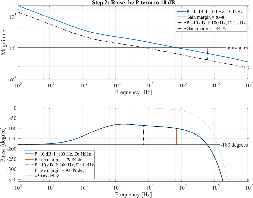
Raise proportional gain to 10 dB
With the introduction of the 1 kHz differentiator, the phase margin improves significantly in the frequency range from 1 to 100 kHz, and the gain margin reaches 84.79. This provides ample room to increase the proportional gain and enhance the open-loop gain while maintaining system stability. A 20 dB increase in proportional gain is acceptable, as it would reduce the gain margin to 8.479 and shift the unity gain frequency to approximately 60 kHz, which still falls within the stable operating range. As a result, both gain and phase margins remain sufficient, and the loop gain increases by 20 dB. The updated OLTF is plotted in Figure 23, where the revised gain and phase margins are also indicated.
Move integrator and differentiator frequencies higher
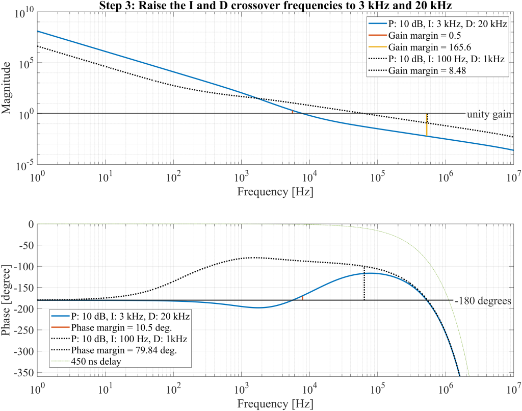
To further enhance the low-frequency gain, the integrator and differentiator gains can be increased, as the available phase headroom between 1 and 100 kHz allows for such a trade-off without significantly impacting the phase margin at higher frequencies. In this configuration, the integrator crossover frequency is raised to 3 kHz and the differentiator crossover frequency to 20 kHz, resulting in a further increase in low-frequency loop gain.
The updated OLTF is shown in Figure 24, where both the gain and phase margins are annotated. These margins are now limited, suggesting the system may become unstable. By examining the transfer function, it is observed that the unity gain frequency shifts to 8 kHz due to the raised differentiator crossover frequency. However, at approximately 100 kHz, the phase remains well above the critical -180° threshold, indicating that additional proportional gain can be applied to push the unity gain frequency higher and recover phase margin.
It is important to note that the OLTF crosses the -180° phase multiple times, leading to multiple gain margins, with only the two margins closest to the critical instability point, where \(G(s)=-1\), being of primary interest. Increasing the proportional gain causes \(|G(s)|\) to move further away from unity near 5.6 kHz, while simultaneously bringing it closer to unity near 528 kHz. This shift introduces a tradeoff between the gain margins on either side of the unity gain frequency.
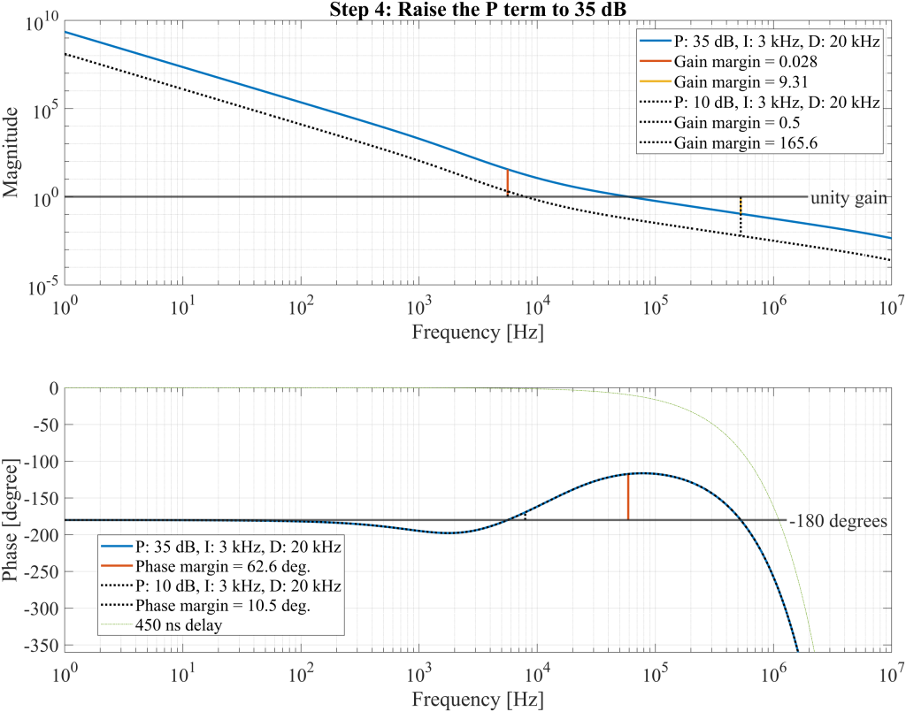
Raise proportional gain to 35 dB
With the understanding that increasing the proportional gain can improve both loop stability and gain, the proportional gain is raised to 35 dB, representing a 25 dB increase. This adjustment shifts the unity gain frequency to approximately 70 kHz, resulting in a more favorable phase margin while also balancing the two gain margins on either side of the unity point. The updated open loop transfer function is shown in Figure 25. It now exhibits a phase margin of 62.6° and two gain margins of 0.028 and 9.31, indicating the system has an appropriate safety margin from \(G(s)=-1\).
Stability analysis with Nyquist criteria
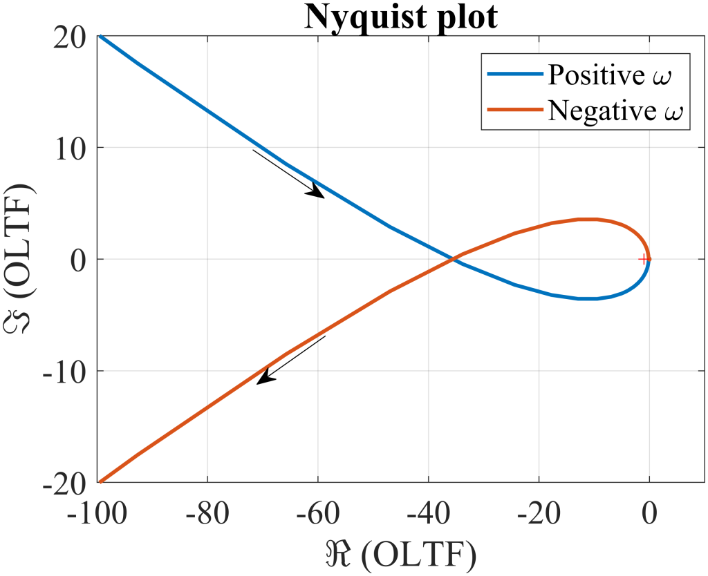
In Figure 25, it is observed that the phase response crosses the 180° point twice. One of these crossings, occurring around 5.6 kHz, corresponds to a gain \(|G(s)|\) greater than one. This condition can lead to positive feedback at that frequency, potentially amplifying noise and causing instability. To assess the stability of the system more rigorously, it is essential to analyze the poles of the closed loop system. Recalling the basic closed loop expression, the system’s output-to-input transfer function is given by \(H(s)= \frac{G(s)}{1+G(s)}\), so the poles of \(H(s)\) are the zeros of \(1+G(s)\).
A useful method for this analysis is the Nyquist plot, which evaluates the OLTF \(G(s)\) along a contour that encloses the entire right half of the s plane. This approach is especially valuable for systems that include a pure delay \(e^{-\tau s}\), since such delays are transcendental and cannot be accurately represented using lumped element models. While a full explanation of the Nyquist criterion is beyond the scope of this note, many resources explain it thoroughly—Chapter 3 of A Guide to Feedback Theory by Joel L. Dawson is a good place to begin.
To apply the Nyquist criterion, let P represent the number of poles of \(G(s)\) in the right half of the s plane, and N denote the number of encirclements around the critical point \((-1,0j)\). Then Z, the number of zeros of \(1+G(s)\) in the right half plane, satisfies the relationship \(N=Z-P\). Therefore, by determining the number of right half plane poles in \(G(s)\), and counting the encirclements of \((-1,0j)\), one can directly infer the stability of the closed-loop system.
Figure 26 presents the Nyquist plot for the system, with the critical point \((-1,0j)\) marked by a red cross. The plot shows one counterclockwise encirclement of \((-1,0j)\) in Figure 25, which suggests potential instability. However, due to the presence of two pure integrators in the loop—one from the VCO’s frequency to phase conversion and the other from the PID controller—the plot extends to infinite radius, making quantitative analysis infeasible. The system must also be evaluated using a qualitative method.
As the complex frequency variable s rotates 180° counterclockwise around the origin in the s plane, the two integrators represented by poles at the origin contribute a total of 360° of clockwise phase shift at infinite radius in the Nyquist plot. This produces one clockwise encirclement that cancels the initial counterclockwise encirclement, resulting in a net encirclement of zero.
Since the OLTF has no poles in the right half s plane and the total encirclement of the point \((-1,0j)\) is also zero, the closed-loop system has no poles in the right half of the s plane. Therefore, the optimized system remains stable.
Open-loop transfer function of the optimized loop
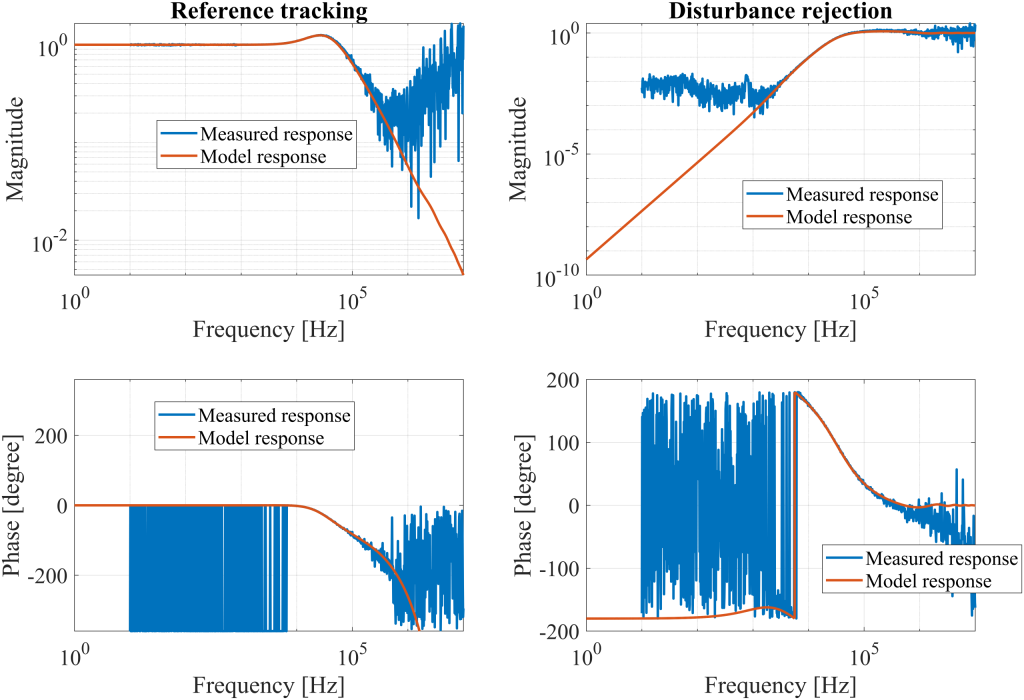
After optimizing the OLTF and verifying the stability of the closed-loop system, the PID controller is configured with a proportional gain of 35 dB, an integrator crossover frequency of 3 kHz, and a differentiator crossover frequency of 20 kHz. The system is then measured to validate the model. Figure 27 displays both the measured and simulated OLTF, while Figure 28 shows the system’s reference tracking and disturbance rejection. The measured results closely match the model predictions.

Noise characterization
This section evaluates frequency noise using the same Moku:Pro device, with the internal clock serving as the reference; thus, any jitter or phase noise from the clock itself is excluded from the measurements. To reduce the influence of sensor noise on the frequency noise analysis, an out-of-loop frequency sensor is used. In this configuration, the primary source of sensor noise is the analog-to-digital converter (ADC). As shown in Figure 29, the VCO output is divided into two separate paths to enhance measurement accuracy: one path is sent to ADC Input 1 to generate the error signal for the feedback loop, while the other is routed to ADC Input 3 and the Phasemeter, which serves as an independent out-of-loop sensor for measuring the VCO’s frequency noise.
Frequency noise was measured under three conditions: free-running, locked with a PI controller, and locked with the optimized PID controller. The time-domain results are shown in Figure 30. The optimized PID controller achieves a peak-to-peak frequency noise of approximately ±20 Hz, approaching the noise floor of the Phasemeter (indicated by the purple line).
This performance is achieved because the control loop attenuates disturbances by a factor of one over \(\frac{1}{1+G(s)}\). In the optimized configuration, the loop gain is sufficiently high to effectively suppress the noise in the loop, including environmental vibrations and temperature variations that could affect the VCO frequency.
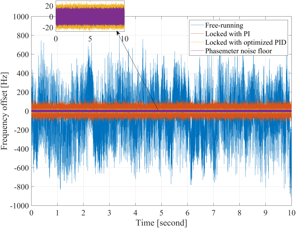
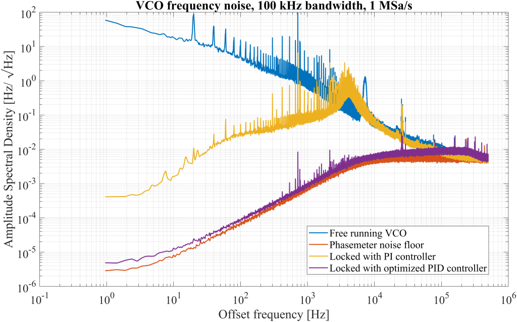
Figure 31 presents the ASD of the measured frequency noise. The purple trace, corresponding to the optimized PID controller, closely aligns with the Phasemeter’s noise floor, indicating that the system is operating near its performance limit. The absence of pronounced noise peaks further confirms that the optimized open-loop transfer function provides sufficient phase margin, ensuring stable and well-damped behavior.
Summary
This application note details the analysis and optimization of a PLL system comprising a VCO and a Lock-in Amplifier equipped with an internal PID controller. By systematically tuning the proportional, integral, and derivative components, the OLTF \(G(s)\) was shaped to maximize loop gain while preserving adequate phase and gain margins to ensure stable operation. System stability was confirmed using the Nyquist criterion, verifying the absence of right-half-plane poles in the CLTF \(H(s)\).
Experimental validation included a comparison between measured and simulated OLTF, with the results showing close agreement. Frequency noise performance was assessed under three operating conditions: free-running, locked with a PI controller, and locked with the optimized PID controller. The optimized configuration achieved performance close to the Phasemeter noise floor, demonstrating its effectiveness in suppressing external disturbances such as mechanical vibrations and temperature-induced frequency drifts.