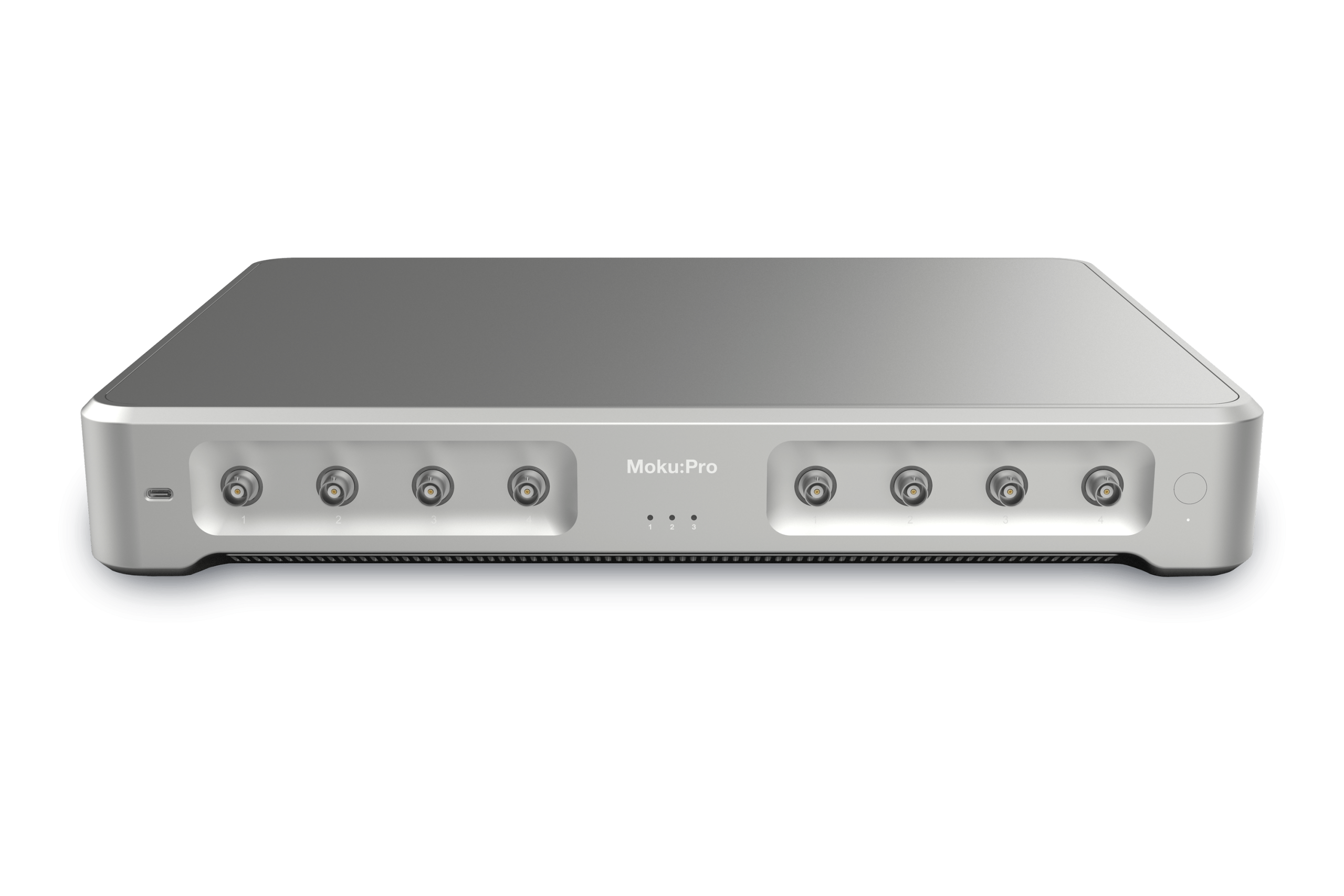
In test and measurement, flexibility has typically demanded tradeoffs in performance. Moku:Pro overcomes these tradeoffs by using signals from a 5 GSa/s, 10-bit ADC, and a 10 MSa/s, 18-bit ADC in a patented blending scheme to deliver a low noise floor and high dynamic range from 10 Hz to 600 MHz. This is achieved through a digital crossover network consisting of balanced high- and low-pass filters that implement real-time blending of the dual ADC data streams.
Analog front-end design and traditional tradeoffs
A critical part of modern digital test instrumentation is having a high-quality analog front end since front-end performance sets a fundamental limit on the fidelity of downstream analysis, processing, and logging of the digitized signals. But selecting an analog-to-digital converter (ADC) typically involves making tradeoffs, such as sacrificing long-term stability for high bandwidth. Figure 1 shows example noise spectra of two ADCs optimized for different signal frequencies.

Figure 1: The noise spectra of two ADCs demonstrating noise increasing at high and low frequencies (1/f noise) along with a white noise level. The spectra of ADCs optimized for high-frequency signals (red) and low-frequency signals (blue) are shown.
Traditionally, when a piece of test equipment is designed for a single function or application, these tradeoffs can be balanced by selecting an ADC optimized for the specific measurement requirements and signal characteristics. In contrast, while the versatility of software-defined instrumentation poses an opportunity to address a diverse range of applications, designing an analog front-end that can meet them all is a challenge. More specifically, Moku:Pro was designed to address a wide set of measurement scenarios, which a single ADC would not be optimized for.
A new FPGA-Based Processing Technique for High-Quality Signal Construction Across the Frequency Spectrum
Realizing the full potential of modern software-defined instrumentation requires a modern approach. Moku:Pro’s front end incorporates two high-performance ADCs. A 5 GSa/s, 10-bit ADC with exceptional bandwidth and high-frequency noise is paired with a 10 MSa/s, 18-bit ADC optimized for low-frequency acoustic signals. A digital crossover network consisting of balanced high-pass and low-pass filters implements real-time blending of the ADC data streams to deliver a low noise floor and high dynamic range from 10 Hz to 600 MHz.
Implementing these filters digitally on the same clock domain gives exceptional control over the filtering characteristics but requires substantial processing power (100s of Giga-operations per second). Fortunately, Moku:Pro’s powerful FPGA (a Xilinx Ultrascale+ system on chip) is up to the task and can combine the data streams in real-time with no discernable effect on latency using only a tiny fraction of its resources. The result is a single seamless data stream with an optimal signal-to-noise ratio across all Fourier frequencies. Thus, a major challenge of software-defined instrumentation is solved by one of its strongest traits: powerful, real-time signal processing.
But How Does it Really Work?
Minimizing the overall noise is important, but a key consideration when designing the filtering network is preserving a unity-gain frequency response for the signal. Figure 2 shows one simple way to achieve this by using the same digital filter structure in both paths before blending. The signal from the BNC connector appears at the left of the diagram before forking to both a high-speed (upper path) and low-speed (lower path) ADC. The upper path is high-pass filtered by 1-TF(f), where TF(f) is the transfer function of the low-pass filter. The bottom path experiences a simple TF(f) transfer function. The recombined signal has a total input-output transfer function of 1-TF(f) + TF(f) = 1 and thus unity gain. As both filters are implemented digital, they are perfectly matched.

Figure 2: A block diagram showing a clarified implementation of frequency-dependent ADC blending with a unity-gain transfer function.
The filtering network is also complicated by the fact that the ADCs are operating with different sample rates. The data streams must be appropriately up- or down-converted before they are combined to reduce the appearance of artifacts in the blended data stream. An additional consideration introduced by different ADC sample rates is anti-aliasing. In general, analog anti-aliasing filters are present at the input of each ADC and the impact of their frequency response on each signal path must be accounted for. Figure 3 shows a simplified block diagram for this situation. The impact of an anti-aliasing filter (not shown) on the high-speed path can be ignored. In this scenario the analog low-pass filter must be matched by a digital low-pass filter. Fortunately, the flexibility of digital filters allows close matching to most common analog filter types. In Moku:Pro’s FPGA, this filter can even be tailored to the individual characteristics of the analog filter, which can differ from unit to unit due to component tolerances, at the time of calibration.
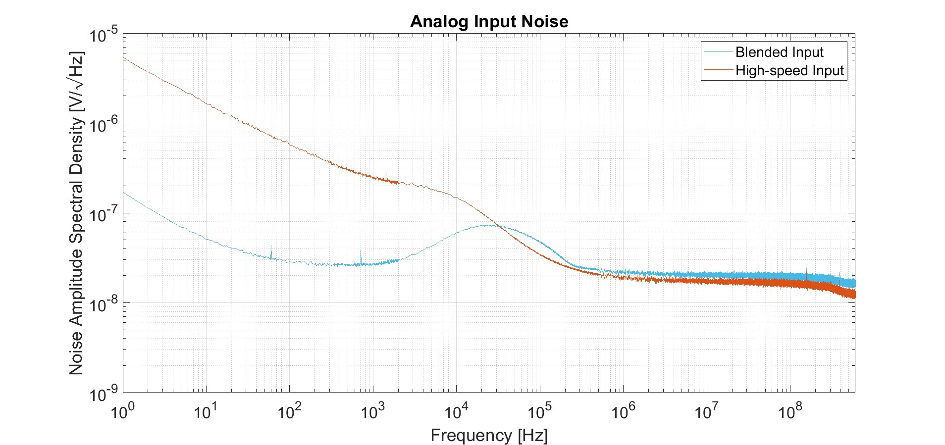
Figure 3: A blending network that compensates for the analog antialiasing filter in the low-speed path with a matching digital low-pass filter in the high-speed path.
Summary
Our FPGA algorithms automatically and intelligently blend the high-speed and low-speed signals from the two ADCs. The user does not need to manually decide which ADC is best to use; instead, data from both are simultaneously acquired and blended to construct an optimal signal for measurement or further processing. This new approach reduces the types of noise and errors commonly introduced when using a single ADC that may not be optimized for the frequencies of interest. For the first time, engineers and researchers do not need to choose between high speed and high precision when acquiring data thanks to Moku:Pro’s blended ADC technology.
Learn more about Moku:Pro.
Have questions or want a printable version?
Please contact us at support@liquidinstruments.com
