This lab tutorial walks through a common power electronics lab to show how the Moku:Go’s Oscilloscope, Waveform Generator, and Power Supplies can be used simultaneously to power and analyze a Buck (Step Down) Converter.
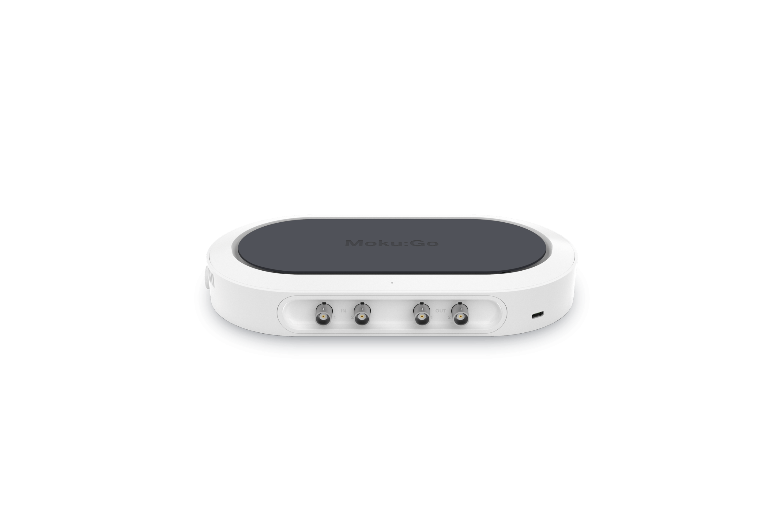
Moku:Go
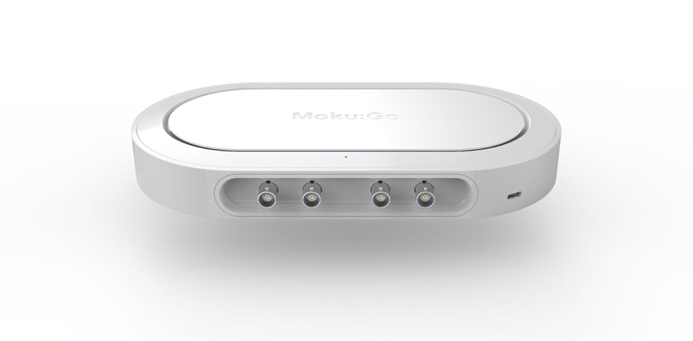
Moku:Go combines 15+ lab instruments in one high performance device, with 2 analog inputs, 2 analog outputs, 16 digital I/O pins and optional integrated power supplies.
Introduction
DC/DC power converters are one of the most common electronic systems implemented today, so being able to quickly debug and evaluate the quality of a converter is important for any kind of engineer. Moku:Go is a great test and measurement device for power electronics because it integrates various instruments into a single environment that allows for rapid circuit development, testing, and validation.
This first converter lab will show how Moku:Go’s integrated Oscilloscope, Waveform Generator, and Programmable Power Supplies (PPSUs) are used to easily characterize a typical buck converter built on a breadboard. Moku:Go is controlling the input power, PWM duty cycle, and PWM frequency for this converter while allowing two input channels for the Oscilloscope. This allows for design changes to be quickly implemented and verified within the same laptop interface to help reduce development time.
Experimental Setup
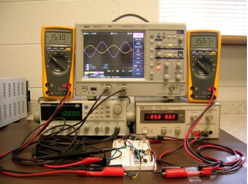
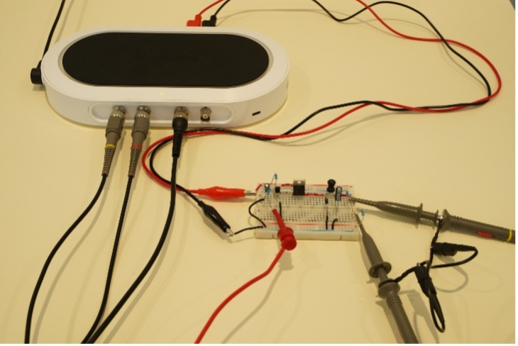
Lab Equipment Setup Comparison
Traditional (left) vs. Moku:Go (right)
Components
- Moku:Go [1x]
- R1 Resistor 1kΩ [x1]
- R2 Resistor 10kΩ [x1]
- R3 Resistor 100Ω [x1]
- R4 Resistor 100mΩ [x1]
- Cin Capacitor 100nF [x1]
- Cout1 Capacitor 100μF [x1]
- Cout2 Capacitor 470μF [x1]
- L1 Inductor 100μH x[1]
- Q1 MOSFET IRFZ44N [x1]
- Q2 Transistor S8050 [x1]
- D1 Diode 1N4007 [x1]
- Breadboard [x1]

Figure 1: Buck Converter
This setup uses both the 16V PPSU and the waveform generator (WG) to drive the MOSFET’s gate. The WG is configured to produce a square wave with digital PWM, which makes driving the MOFSET and characterizing the buck converter simple since it is all done from a single interface. The transistor Q2 is used as the gate driver and converts the 5V square wave to a 12V square wave to ensure the FET is operating in its saturation region. Keep in mind, that the driver circuit is inverting the duty cycle of the PWM signal, so an increase in duty cycle in the WG interface translates to a decrease in duty cycle at the MOSFET’s gate.
Lab Procedure
1. Circuit Setup
Construct the circuit in Figure 1 using components from the Experimental Setup section.
Configure PPSU2 to 12V and 150mA. Then, set the integrated Waveform Generator to have a square wave output with VPP = 5V, Voffset = 2.5V, f= 500Hz, and D = 50%. The software setup should look similar to Figure 2 below.
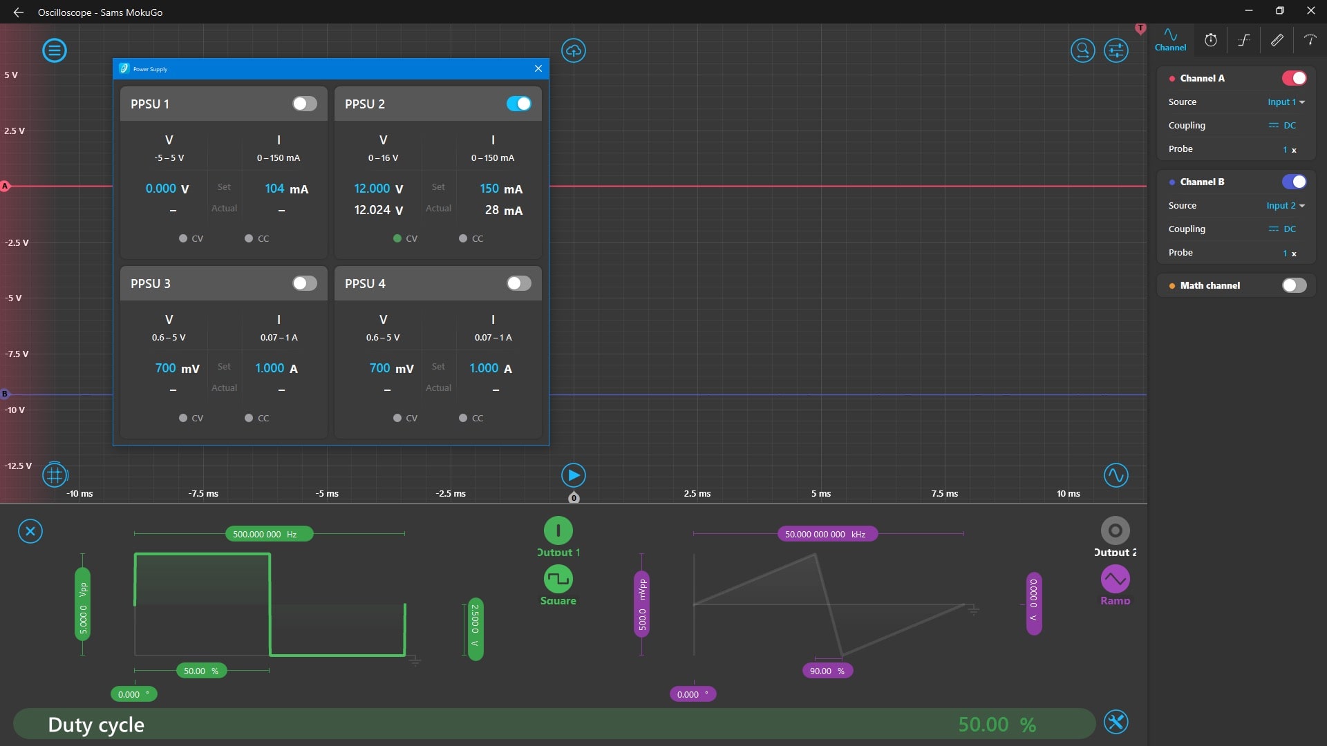
Figure 2: Moku:Go Software Setup
2: Test Gate Driver Signal (VGS)
Connect a scope probe from Input1 to the gate of the MOSFET Q1 and a different scope probe from Input2 to the source (pin 3) of the MOSFET. Keep in mind that every input and output of Moku:Go shares a common ground, so the only ground wire that should be used is the one for the PPSU (black banana plug wire). From here, enable the math channel and select the subtraction operator to subtract Input2 (ChB) from Input1 (ChA). This will give you the VGS waveform.

Vary the duty cycle in the desktop app, does the waveform look how you expect it to? How does varying the duty cycle in the desktop app change the duty cycle of the measured VGS waveform?
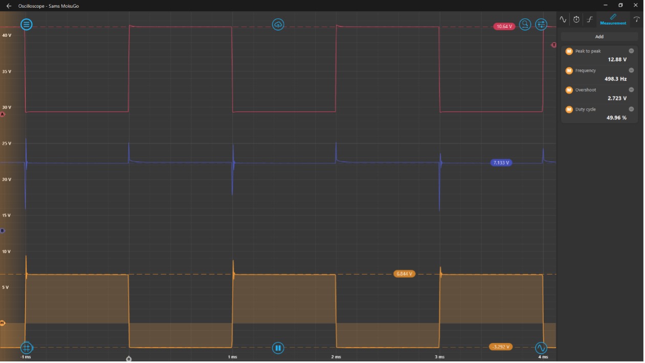
Figure 3: VG waveform using the Math channel
Typical points of interest for VGS are the rising and falling edges of the PWM signal to ensure voltage overshoot does not break the FET’s gate. Zoom in to the rising edge of one pulse using the magnifying glass button in the top right, or enable rubber-band zoom by pressing ‘R’. You can also use the mouse wheel scroll to vary the time divisions and ctrl+scroll to vary voltage divisions.

Once focused on the waveform of interest, we can measure the voltage overshoot using the draggable cursors from the bottom left cursor button. Drag up from the ![]() button for voltage cursors and drag right for time cursors. There can be up to 8 total cursors on screen at once and each of them contains additional functionality like tracking max/min or being set as reference. To access the smart cursor menu, right-click on the number pill on the Oscilloscope screen. You can see that the grey time-axis cursors are measuring the turn-on time of the FET with the leftmost one being set as a reference. This tells us our FET has a turn-on time of about 25.5µs.
button for voltage cursors and drag right for time cursors. There can be up to 8 total cursors on screen at once and each of them contains additional functionality like tracking max/min or being set as reference. To access the smart cursor menu, right-click on the number pill on the Oscilloscope screen. You can see that the grey time-axis cursors are measuring the turn-on time of the FET with the leftmost one being set as a reference. This tells us our FET has a turn-on time of about 25.5µs.
You can also use the automatic measurements in the ‘Measurement’ tab located in the settings drawer on the right side of the screen. Click on the measurement to change its type, channel, or to set a difference channel measurement.
What is the voltage overshoot at the gate terminal when the FET turns on and is it above the maximum VGS rating on the datasheet?
[Solution]
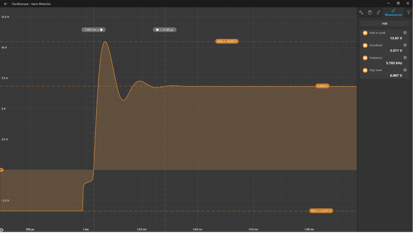
Figure 4: VGS Overshoot and oscillations measurement
We can see our overshoot voltage peak is about 10.48V. Looking at the IRFZ4NN data sheet, we see it is not large enough to damage the FET’s gate (±20V).

Figure 5: IRFZ4NN VGS Max rating
3: Converter Efficiency
The most common figure of merit for any type of power converter is its efficiency, given as a ratio of Pout/Pin, where Pout = Vout*Iout and Pin = Vin*Iin. What is the converter’s efficiency at D = 50%?
[Solution]
Since Moku:Go is being used to both power the converter’s input and monitor the output, it is straightforward to get a power efficiency measurement by using the PPSU ‘Actual’ measurements and the Oscilloscope’s Math channel. Measuring the voltage across the load resistor R3 and the voltage across the shunt resistor R4, the Math channel can then be enabled and set to its function mode. This way, you can enter the power equation directly using Channel A as the output voltage and divide the voltage on Channel B by the shunt resistor (in this case R4 = 100mΩ). You can also choose the desired units in this mode for the Math channel as well. Adding a ‘Mean’ measurement to the measurements tab will then give us Pout. To get Pin, we simply need to open the PPSU window and multiple Vactual by Iactual. This gives us a converter efficiency of…

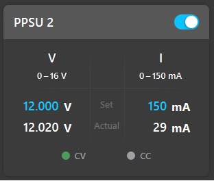
Figure 6: PPSU 2 Power Monitor to obtain Pin
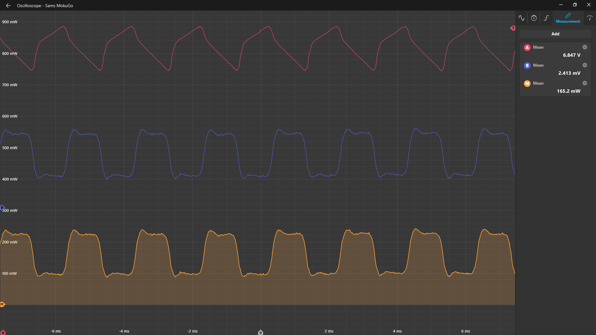
Figure 7: Oscilloscope Setup to obtain Pout
4: Vout Ripple Voltage
Set D = 0.3 and enable AC coupling. Measure the output ripple of Vout across R3. If you are having trouble getting a clean measurement, enable precision mode in the ‘Acquisition’ settings tab. Enable averaging to help with repeated measurements as well.
What is the RMS value of Vout ripple voltage?
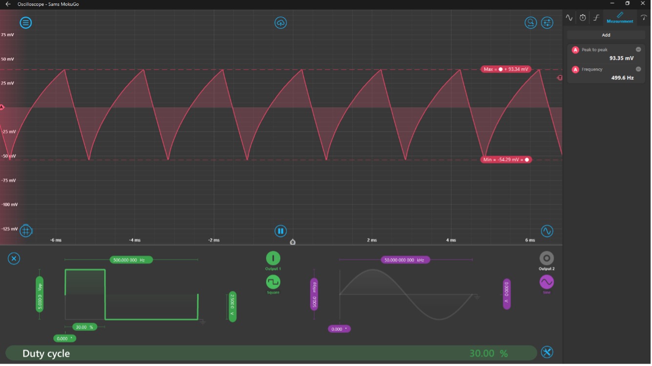
Figure 8: Vout Ripple with Cout1 = 100µF
We can see that our peak-to-peak ripple voltage is about 93mV, which isn’t too great. Now change the Cout capacitor to Cout2 = 470µF. Is the ripple reduced?
[Solution]
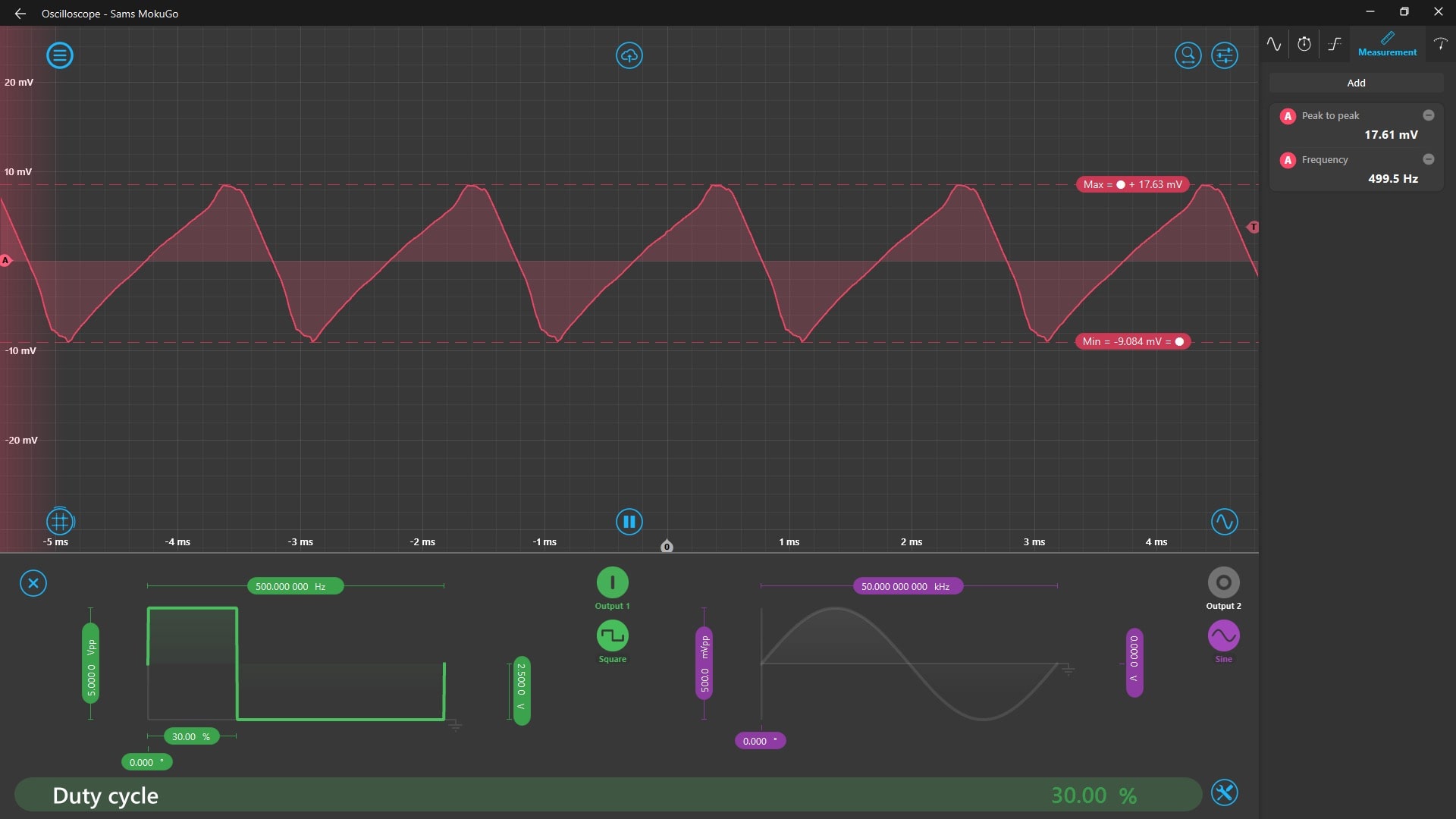
Figure 9: Vout Ripple with Cout2 = 470µF
5: Vout Harmonics
Enable the Math channel and use FFT to determine magnitude of frequency components.
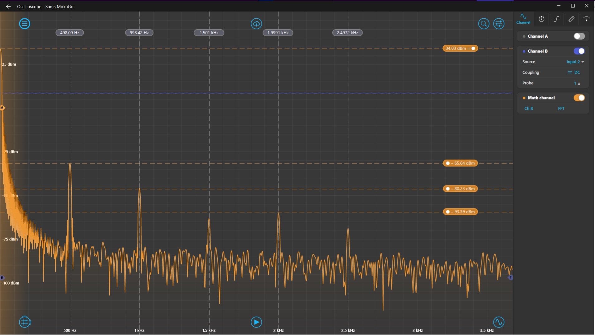
Figure 10: Vout FFT
6: VDS Ripple Current
With Cin disconnected, connect scope probes across VDS. Remember not to use the grounding pins of the scope probes and instead use the Math channel to obtain the VDS waveform. What is the frequency of the oscillation when the switch closes? Is overshoot acceptable?
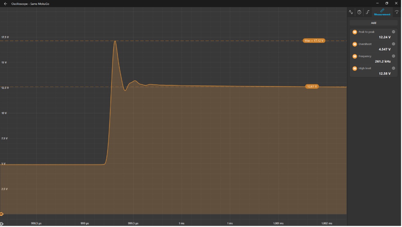
Figure 11: VDS without Cin
Now connect Cin and see how it changes the ripple current waveform.
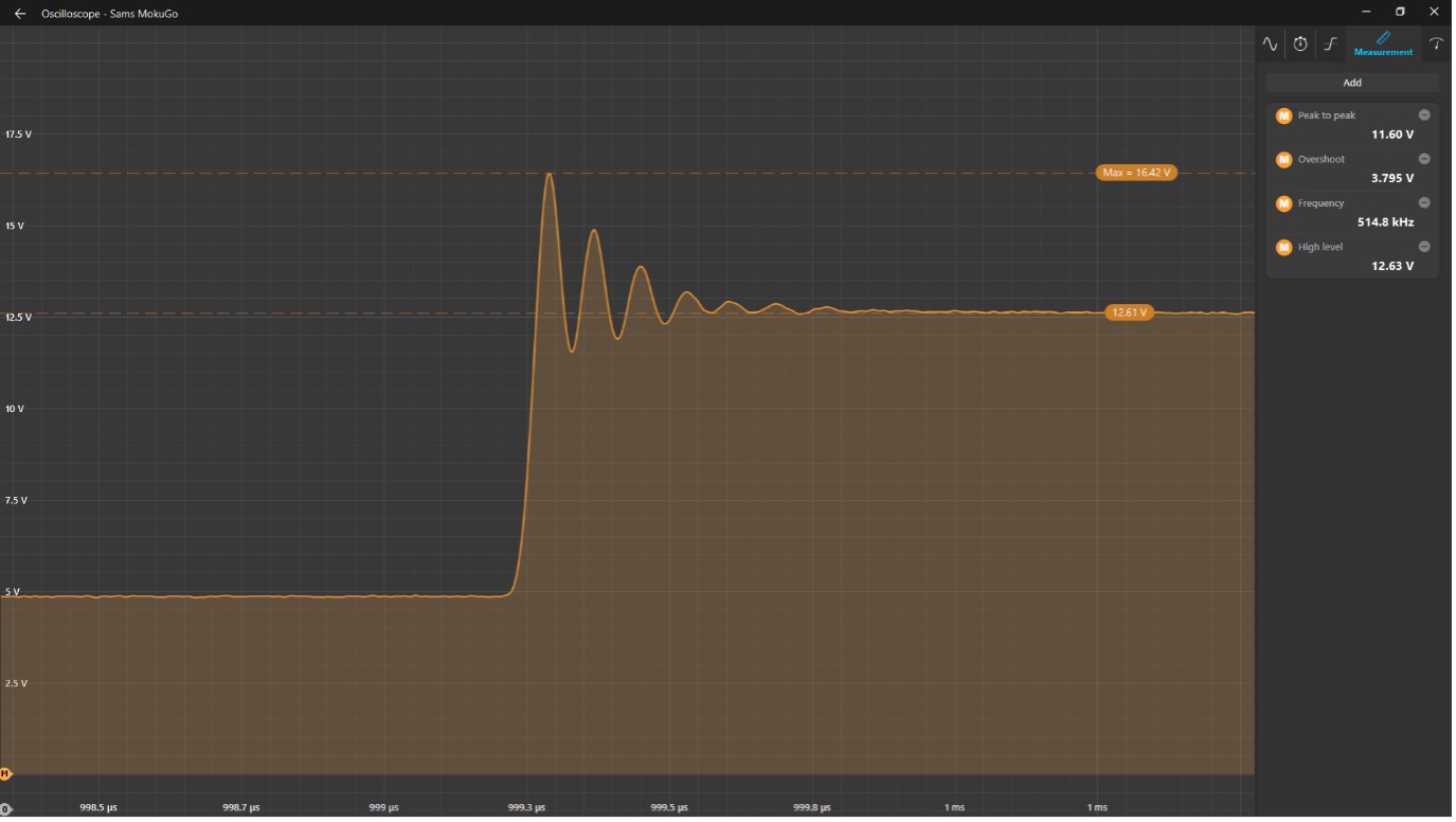
Figure 12: VDS with Cin
We can see that Cin trades off a reduction in peak overshoot voltage for increased ringing during MOSFET turn-on time.
7: VL in Discontinuous Conduction (DCC)
Set D = 10% and connect a scope probe across L1, this is your VL. What is the frequency of the parasitic oscillation?
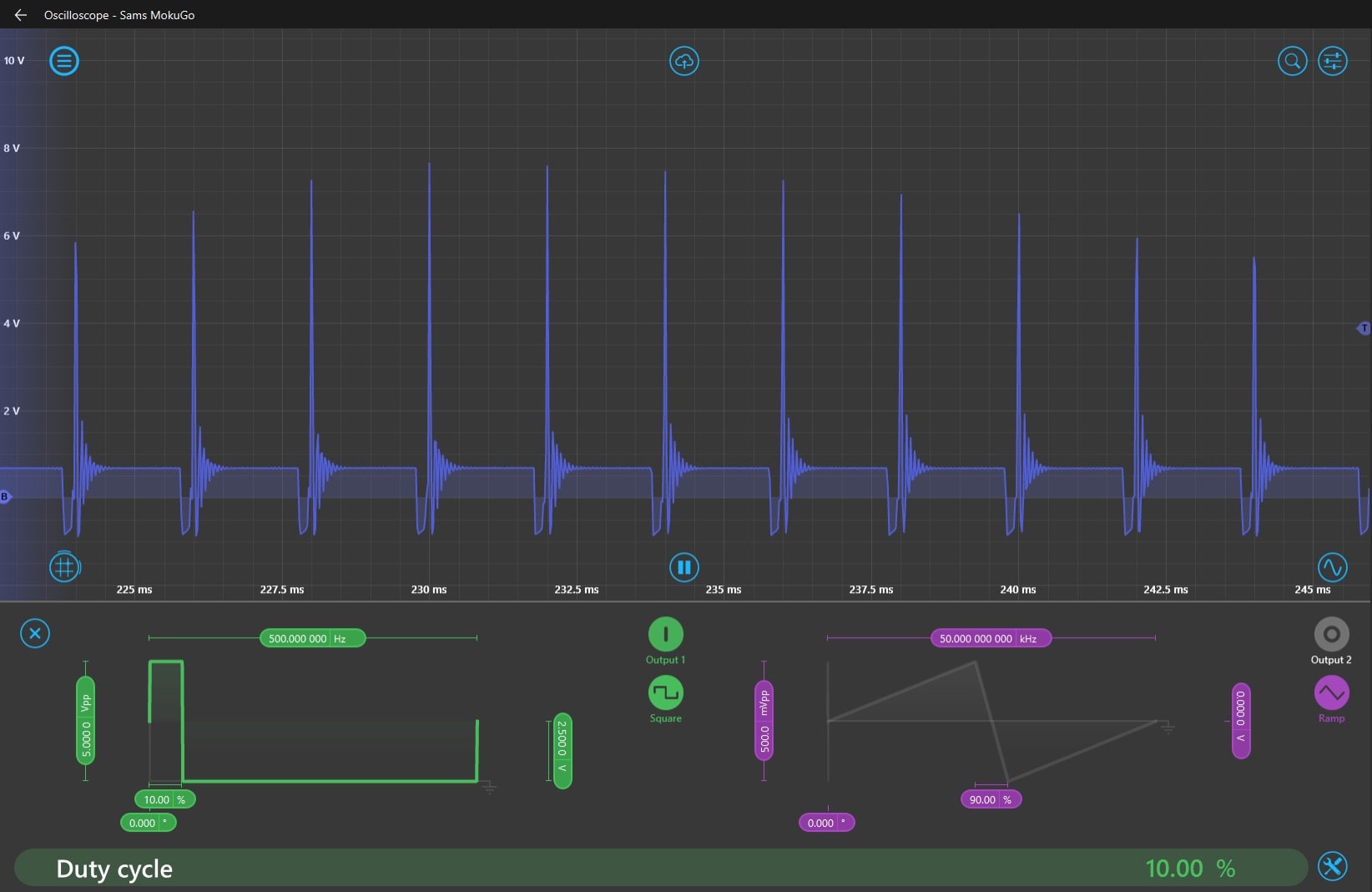
Figure 13: VL oscillations
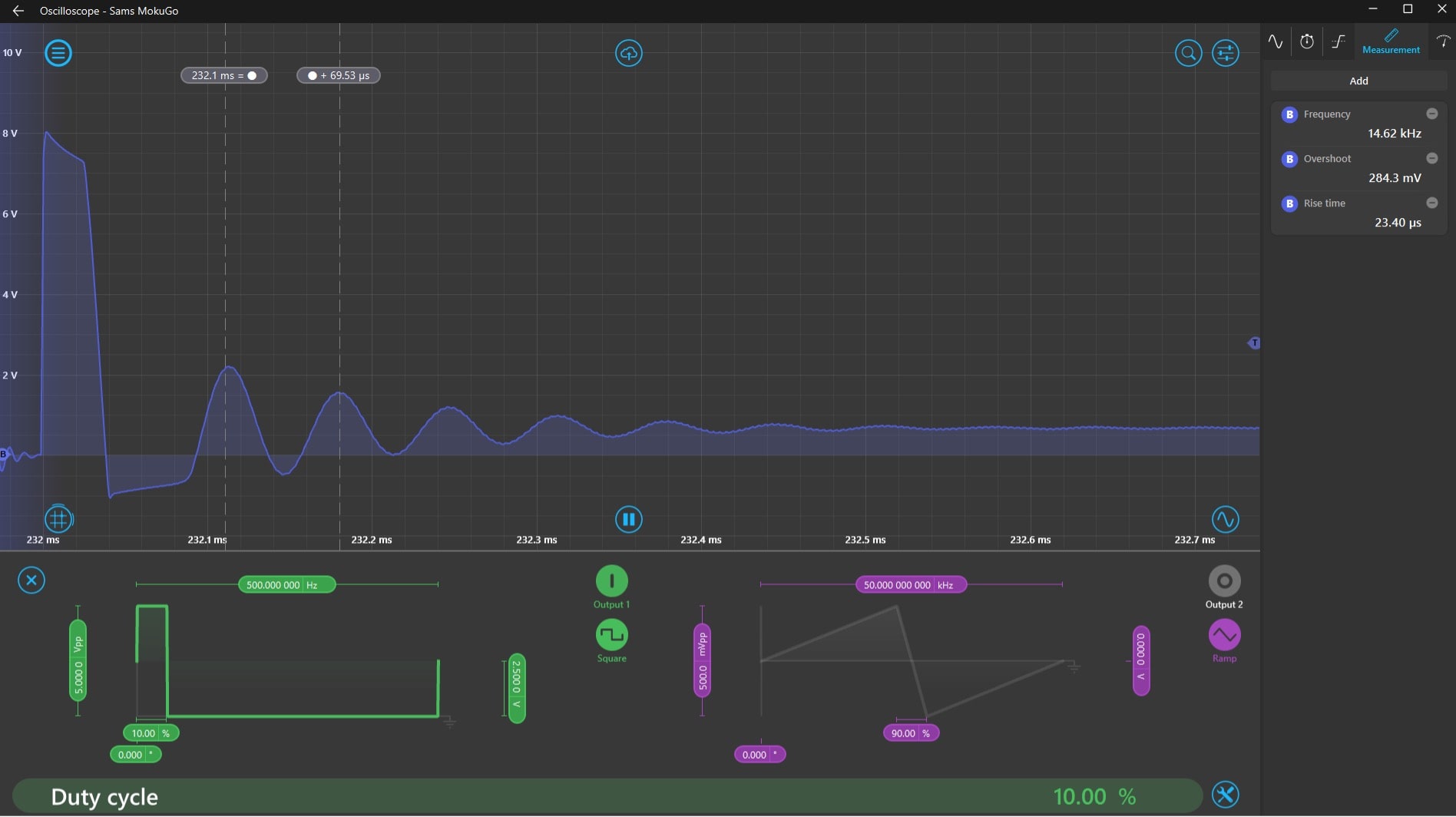
Figure 14: VL oscillations
Finally, let’s see how frequency impacts the converter’s DCC mode. Set D = 80% and slowly increase the frequency in the integrated WG by selecting the frequency settings box and using the arrow keys to increase the frequency. The significant digit the cursor is in front of is the digit the arrow keys will change.
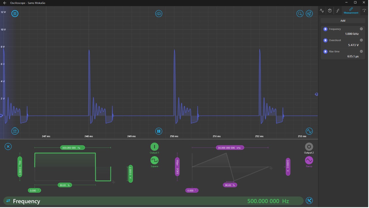
Figure 15: VL in DCC @ 500Hz
We know that the converter is no longer operating in DCC when these oscillations are not present in the VL waveform. At around 4.3kHz, the converter returns to continuous conduction mode. This type of active learning style can be great for teaching students why component selection is important for desired device operation.
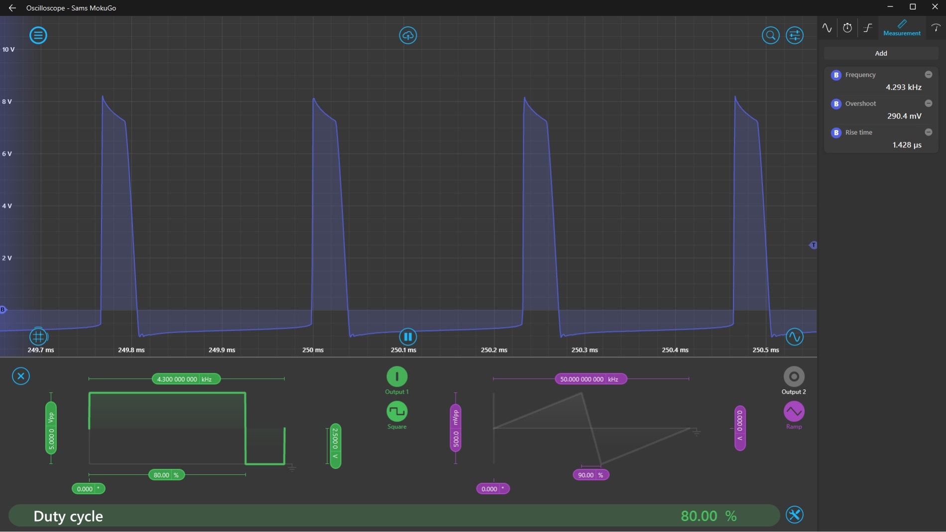
Figure 16: VL in CC @ 4.3kHz
Summary
This lab goes through a typical buck converter analysis for undergraduates while focusing on how to use the integrated instrument environment of Moku:Go to quickly get the converter running and then do a basic performance analysis. The ability to vary the converter’s duty cycle and switching frequency while viewing specific waveforms in the integrated oscilloscope environment allows students to easily see how these parameters affect the performance of a converter. It can also be great for quickly comparing converter performance against different components since the power supplies are also accessible from the same interface and screenshots of converter performance can be quickly saved since the scope and controls are already on your computer.
Benefits of Moku:Go
For the educator & lab assistants
Efficient use of lab space and time
Ease of consistent instrument configuration
Focus on the electronics, not the instrument setup
Maximize lab teaching assistant time
Individual labs, individual learning
Simplified evaluation and grading via screenshots
For the student
Individual labs at their own pace enhance the understanding and retention
Portable, choose pace, place, and time for lab work be it home, on-campus lab, or even collaborate remotely
Familiar Windows or macOS laptop environment, yet with professional-grade instruments
Moku:Go Demo Mode
You can download the Moku:Go app for macOS and Windows at the Liquid Instruments website. The demo mode operates without the need for any hardware and provides a great overview of using Moku:Go.
Have questions or want a printable version?
Please contact us at support@liquidinstruments.com
