Evaluation of a test instrument often revolves around its noise floor, a critical metric for high-precision instruments. However, establishing a clear link between noise floor and the quality of measured signals can be elusive. This application note aims to clarify the concept of noise spectral density and explores diverse factors that can significantly increase measured signal-to-noise ratios, utilizing the Moku:Pro.
Understanding the noise floor
When considering the acquisition of a test instrument, the noise floor represents a critical criterion due to its significant impact on measured signal-to-noise ratio (SNR) and its direct influence on the capability to detect weak signals. Analog noise originates from various sources, including electromagnetic interference (EMI) and analog-to-digital converter (ADC) quantization, resulting in a complex composition of noise components. This application note provides an analysis of the noise floor, exploring the impact of noise bandwidth on noise power and the SNR of the measured signal.
SNR is a dimensionless measure that evaluates the ratio of signal power to noise power, serving as a key parameter in assessing signal acquisition and processing systems.
SNR = \(\frac{P_S}{P_N}\, (1.1) \)
Signal power PS is computed using Eq. 1.2, where T represents the duration of an observation interval. For periodic signals, T equals the period of the signal, and PS corresponds to the mean square value of the signal.
\(P_s = \frac{1}{T} \int_{0}^{T} s^2 \, (t) dt \ = E[s^2 (t)], (1.2)\)
For sinusoidal signals, the root mean square (RMS) amplitude is A/√2, where A denotes the amplitude of the sinusoidal signal. And the power of the sinusoidal signal is A2/2.
Noise power PN can be calculated using the same method.
\(P_N=\frac{1}{T} \int_{0}^{T} n^2 \, (t) dt = E[n^2 (t)]=[(E[n(t)])]^2+E[(n(t)-E[n(t)])^2 ]=\mu^2+ \sigma^2 , (1.3) \)
When the noise’s DC offset, μ, is zero, PN is equal to the variance, σ2, of the noise.
Consider an experiment using a sine wave signal with an amplitude of 10×√2 mV, corresponding to an expected power of 100 μV2. Gathering data in different noise environments leads to distinct levels of additional noise power and, therefore, SNR. In Figure 1, we depict the outcomes observed under four different noise conditions.
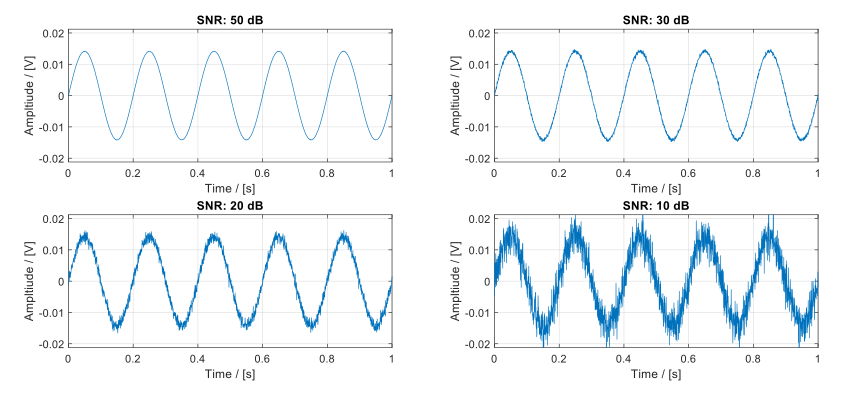
Figure 1: Simulation of a constant-power sine wave captured under multiple additive noise power scenarios, resulting in SNR values ranging from 50 dB to 10 dB.
In the plots shown in Figure 1, while the signal remains constant, the additive noise power changes. As the noise power increases, the signal’s visibility decreases. Eventually, when the noise becomes substantial, it entirely masks the signal, as shown in Figure 2.
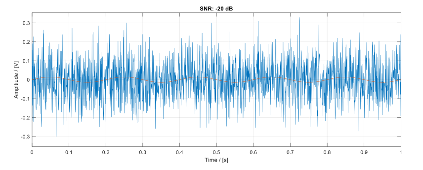
Figure 2: A noisy environment leading to a measured -20 dB SNR (blue). The sine wave (red) is unable to be distinguished from the blue trace.
This implies that excessive noise generated by the instrument could obscure the subtle, yet crucial, signals. For instance, in a single-photon experiment, the signal may be obscured by the analog input noise. The following sections will further investigate this noise floor and explore possible strategies to improve SNR.
Quantization noise
The term “noise level” encapsulates various noise sources like thermal noise and quantization noise, leading to diverse noise behaviors, including 1/f flicker noise and white noise. Analyzing the noise floor involves examining both the time and frequency domains.
Figure 3 shows a typical plot of the noise floor (blue line) and the signal with the additive noise floor (red).
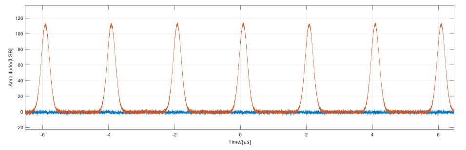
Figure 3: Time-domain noise floor (blue) and the actual input signal (red) captured by the Moku:Pro ADC.
Focusing on the time domain offers valuable insights into the RMS noise power and the distribution of noise amplitude. Figure 4 displays the statistical properties of the noise floor collected in Figure 3, demonstrating that the input noise closely follows a Gaussian distribution with a mean value of -0.7095 least significant bits (LSB) and a standard deviation of 1.1472 LSB.
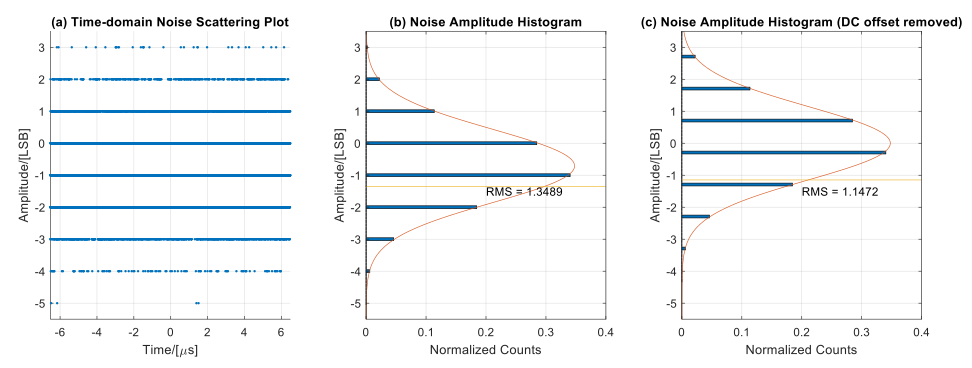
Figure 4: The statistical distribution of ADC noise is presented in units of LSB. The bar plot (b) indicates an RMS noise of 1.3489 LSB. The DC offset (μ) in the collected noise data is -0.7095 LSB. After removing the DC offset, the RMS value is 1.1472 LSB, as shown in plot (c). This relationship is verified by the equation 1.34892 -1.14722=(-0.7095)2
In this section we delve into the analysis of quantization noise. Often, concerns arise regarding the resolution of test instrument analog inputs, as quantization noise may distort the measured signal and compromise signal quality. Yet, in high-bandwidth instruments, quantization distortions are typically less significant. This occurs because the white thermal noise, produced by the thermal motion of electrons in the electrical components, can effectively randomize the quantization noise. As a result, the quantization noise integrates into the additive white noise floor rather than appearing as input-correlated harmonic distortions, even though the overall quantization noise power remains unchanged.
When the white thermal noise surpasses quantization noise and its standard deviation exceeds 1/3 of the LSB, the quantization noise can be considered white noise distributed uniformly across the entire frequency spectrum. Otherwise, the quantization noise may appear as harmonic distortions in the frequency domain when an input signal is present. In most high-bandwidth systems, the noise power goes beyond 1/3 of the LSB due to the significant noise bandwidth, despite a low noise floor. The expected quantization noise power calculation follows Eq 2.1, where eq2 represents the instantaneous quantization noise power and E(eq2) is the expectation value of the quantization noise power. This assumes the quantization noise is uniformly distributed across the step resolution range [-1/2 ,1/2 ] in units of LSB. The probability distribution function p(eq) is equal to 1 due to uniform distribution, meaning all values are equally likely.
\((E(e_q^2 )=\int_{-1/2}^{1/2}e_q^2 \, p(e_q) de_q = \frac{1}{12}, (2.1) \), where p(eq) is the probability distribution function of the error distribution within 1 LSB.
The RMS quantization noise power is √(1/12)=0.2887 LSB , significantly lower than 1 LSB in the overall noise contribution. Therefore, quantization noise is not the dominant input noise source and is negligible compared to input white thermal noise. Consequently, quantization noise has a low impact on the SNR of measured signal.
Noise signals are often time-independent, indicating that the statistical characteristics of the system’s input noise, such as mean, noise power, and distribution form, remain stable over time. Additionally, when measuring a signal within a specific frequency range, analyzing noise in the time domain may not directly contribute to understanding the final measured SNR. Therefore, a more meaningful analysis lies in exploring noise in the frequency domain, providing essential information about the distribution of noise power across the entire frequency spectrum via a noise power spectral density (PSD) or amplitude spectral density (ASD).
As discussed above, noise power directly impacts SNR, where the noise floor entails not just the overall power but also the noise power-to-bandwidth connections. When considering the noise floor, a crucial aspect is that noise is a random process, constituting a broadband signal distributed across the entire frequency range rather than specific frequency components. In reality, there might be different noise contributions in the frequency spectrum. For instance, input noise can arise from the non-linearity of the input pre-amplifier and impedance mismatch between the ADC and subsequent circuits. In the context of Moku:Pro, a small hump around 30 kHz is noticeable in Figure 5.
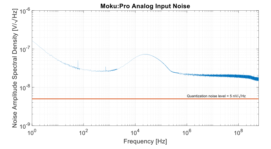
Figure 5: Noise ASD of the analog input of Moku:Pro with a 400 mVpp input range. The minor increase around 30 kHz is attributed to the blending of low- and high-speed ADCs.
To achieve low input-noise across the entire frequency range, Moku:Pro uses two analog inputs — slow and fast. The fast ADC offers low noise in the high-frequency range, whilst the slow ADC exhibits a lower noise spectrum in the low-frequency range. Combining the inputs of both ADCs results in a low-noise spectrum at all frequencies, relative to using either the fast or slow ADC alone.
Figure 5 offers an intuitive demonstration of noise power distribution in the frequency range, providing additional insights into the expected noise power in the measurements. It also facilitates a comparison between the magnitudes of quantization noise and total input noise. The calculation of quantization noise ASD is shown in Eq 2.2, where ∆ is the minimum step resolution, approximately 0.44 mV on Moku:Pro. The Nyquist frequency is 625 MHz, given that the Moku:Pro native sampling rate is 1.25 GSa/s.
\(ASD_{RMS,quantization} = \sqrt{\frac{\Delta^2}{12*625 MHz}} \approx 5 nV/\sqrt{Hz}, (2.2) \)
The averaged compound noise level on Moku:Pro is 17 nV/√Hz, while the noise level, excluding quantization noise, is 16 nV/√Hz. Therefore, the quantization noise has only a limited effect on the input SNR.
Reducing noise power
Improving SNR is always an interesting topic which includes two aspects: lowering the noise floor and constraining noise bandwidth. As observed in prior sections, the noise floor, essentially a noise ASD, underscores the significance of bandwidth in practical experiments. The total noise power results from integrating the single-sided noise PSD S(f) across the noise bandwidth BWN, spanning from the lower to the higher frequency bounds fhigh – flow.
\(P_N= \int_{f_{low}}^{f_{high}} S(f) \, df \approx S(\frac{f_{high}+ f_{low}}{2})\cdot[f_{high} – f_{low} ] \approx N_0\cdot BW_N, (3.1) \)
In a narrow bandwidth, the noise PSD exhibits minimal variation, particularly at high frequencies. Consequently, \(S(\frac{f_{high}+f_{low}}{2})\) can be accurately approximated as a constant single-sided PSD, denoted as N0. Thus, the noise power PN can be expressed as \(N_0 \cdot BW_N\). This suggests the possibility of reducing the noise bandwidth to minimize the noise power in the measured signal. Given that a pure sinusoidal signal, by definition, lacks bandwidth, this implies that the signal power P_signal remains unaffected by changes in 〖BW〗_N as long as the signal frequency is within the range of [f_low,f_high ].
The SNR can be expressed as in Eq 3.2 because P_signal is independent of the bandwidth BWN. As BWN approaches zero, the noise power, \(N_0 \cdot BW_N\), tends toward zero, but Psignal remains constant. Consequently, the SNR can be improved significantly.
\(SNR = \frac{P_{signal}}{N_0\cdot BW_N}, (3.2) \)
Tests on Moku:Pro
This section will utilize two instruments, the Oscilloscope and Lock-in Amplifier, to verify the theory that noise power is directly related to noise bandwidth. The Oscilloscope will showcase the efficacy of noise bandwidth reduction through Precision mode, while the Lock-in Amplifier will employ the embedded lowpass filter to limit the noise bandwidth. The demonstration aims to clarify the connection between noise bandwidth and the noise power of both instruments. Additionally, the Lock-in Amplifier will illustrate the relation between SNR and lowpass filter bandwidth.
Oscilloscope
The Moku Oscilloscope offers two data acquisition modes: Precision and Normal. When adjusting the timebase, the sampling rate automatically changes to accommodate memory depth limitations. However, downsampling can occur in two ways. In Precision mode, full-rate signals from the ADCs are averaged (a form of filtering) to decimate the signal, preventing potential signal aliasing and reducing signal bandwidth. Conversely, Normal mode directly downsamples the full-rate signals without averaging. It may seem counterintuitive, but an oscilloscope with high bandwidth can exhibit poorer SNR performance than a low-bandwidth oscilloscope when measuring a low-frequency signal, assuming both oscilloscopes have the same noise PSD. This is because the high-bandwidth oscilloscope can include a large amount of noise power in the measurements because the BWN is considerable. To address the impact of high noise power caused by increased bandwidth, one straightforward approach is to reduce the measurement bandwidth by decimating the digitized signal. This is the essence of the Precision mode, where averaging is performed on the full-rate signals.
The plot in Figure 6 demonstrates the comparison of the noise power in Normal and Precision modes. It is evident that the noise power in the Precision mode decreases with the reduction of noise bandwidth, aligning with the expected trend of a 10 dB/dec slope. It’s worth noting that the small hump in the measured results indicates a larger noise regime caused by ADC blending shown in Figure 5.
However, the noise power in Normal mode remains unaffected by the noise bandwidth. This phenomenon is explained by the folding back of noise power from higher frequencies into the Nyquist bandwidth (aliasing), forming a nearly flat noise power curve, commonly referred to as aliasing noise power.
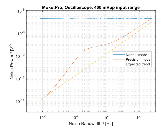
Figure 6: Noise power of collected noise data under various bandwidths using the Moku:Pro Oscilloscope in Normal and Precision modes. In Normal mode (blue), the noise power remains constant due to aliasing noise power, while in Precision mode (red), it aligns with the anticipated noise power trend (orange).
This aliasing of noise power is more evident in the calculated ASD of the collected data shown in Figure 7. In Precision mode, all measured spectra share a consistent noise floor, irrespective of the sampling rate; the only distinction lies in the noise bandwidth corresponding to different sampling rates. Contrastingly, in Normal mode, the noise floor varies with changes in the sampling rate, following a specific rule defined by the following equation:
\(Noise floor = 17 nV/\sqrt{Hz} \cdot \sqrt{\frac{1.25 GSa/s}{Sample rate}}, (3.3) \)
17 nV/√Hz is the mean noise ASD across 625 MHz bandwidth
This implies that the aliasing noise power elevates the noise floor when the signal bandwidth decreases, causing the noise floor to rise above the blending hump and making the blending hump invisible in the Normal mode ASD. Consequently, Normal mode fails to decrease the noise power due to its inability to effectively reduce the noise bandwidth.
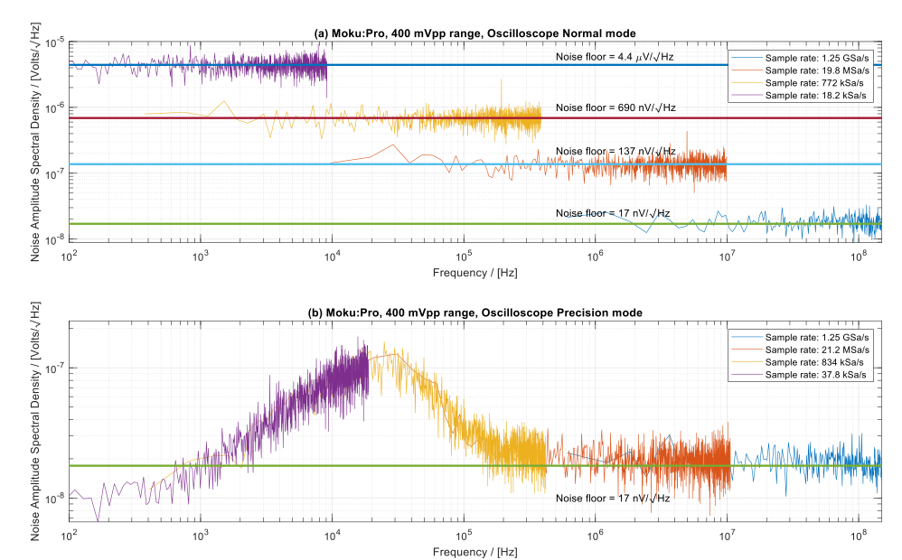
Figure 7: Noise floor variations under different sampling rates, observed through Moku:Pro Oscilloscope in both Normal and Precision modes. In Normal mode (a), noise floors increase as the sampling rate decreases, the total noise power remains constant. In Precision mode (b), the noise floor remains consistent across all sampling rates.
Lock-in Amplifier
The noise reduction technique employed by the Oscilloscope involves averaging and retains signals within the Nyquist bandwidth at the instantaneous sampling rate. While this is a highly efficient method for gaining an intuitive understanding of the input signal, it comes with a notable drawback when handling a high-frequency tone modulated by a narrow bandwidth signal. In such cases, the Oscilloscope must maintain a bandwidth higher than the signal frequency to accurately measure the signal. A high bandwidth entails the presence of significant noise power in the measured data. Additionally, the low-frequency range typically exhibits a high noise floor due to 1/f flicker noise, leading to a low SNR in the measured signal.
In this scenario, a Lock-in Amplifier proves to be a valuable tool for signal acquisition. The operational principle of the Lock-in Amplifier involves down-conversion with a selectable lowpass filter bandwidth. Choosing a small lowpass filter bandwidth effectively limits the noise power while maintaining the integrity of the modulated signal.
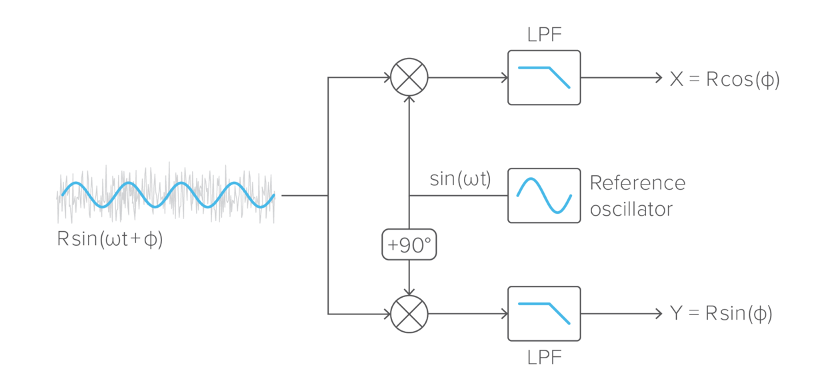
Figure 8: The Moku Lock-in Amplifier features a dual-phase demodulator for measuring both the in-phase and quadrature-phase components. The lowpass filters (LPFs) attenuate the 2ω component and reduce the noise bandwidth.
In Figure 9, Moku:Pro was configured with a 400 mVpp input range, 50 Ω input impedance, and 10 MHz demodulation frequency. The noise data were collected by selecting different lowpass filter corner frequencies to equivalently reduce the noise bandwidth. It can be observed that the measured noise power aligns with the expected noise power curve, exhibiting a 10 dB/dec slope. Furthermore, the noise power curve measured with the Lock-in Amplifier differs from that obtained using the Oscilloscope. The Lock-in Amplifier concentrates on a narrow band in the high-frequency range. Consequently, the noise floor probed by the Lock-in Amplifier remains relatively flat. The `blending’ hump is not encountered, resulting in the measured noise power aligning well with the expected noise power curve.
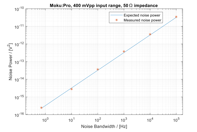
Figure 9: Noise power of recorded data using various lowpass filter corner frequencies. The measured noise power aligns with the anticipated noise power curve, exhibiting a decreasing slope of 10 dB/dec.
The ASD of the gathered data is presented in Figure 10. The roll-off introduced by the lowpass filter is clearly visible in this plot, emphasizing the alignment of the noise bandwidth in the collected data with the corner frequency of the lowpass filter. At high frequencies, the ability to further attenuate noise is constrained by the resolution limitations inherent in the internal signal chain.
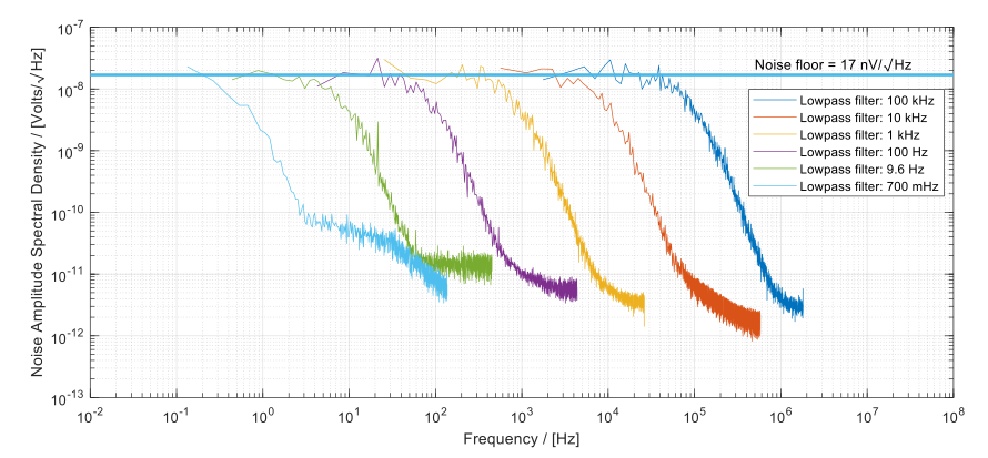
Figure 10: The measured ASD of the recorded data when implementing different lowpass filter corner frequencies. The roll-off point corresponds to the configured lowpass filter corner frequency.
Impact of input range on noise floor
It’s important to note that the noise floor may vary for different input ranges. To delve deeper into this matter, the implementation of input ranges will be discussed in this section. The most direct approach to realizing different input ranges on a hardware platform involves applying attenuations to the analog input frontend. For instance, with a 20 dB attenuation, the equivalent maximum detectable signal without any clipping effects is 10 times larger than in the no-attenuation scenario. In other words, a 400 mVpp ADC can effectively measure a 4 Vpp signal when equipped with a 20 dB attenuator. However, the input noise of the ADC typically remains constant. This implies that the equivalent noise power also increases by a factor of 10 as the input range expands.
In Figure 11, the noise power under three ranges is presented. It is evident that the noise power curves exhibit a 20 dB separation between adjacent lines, signifying an increase in noise power with the expansion of the input range.
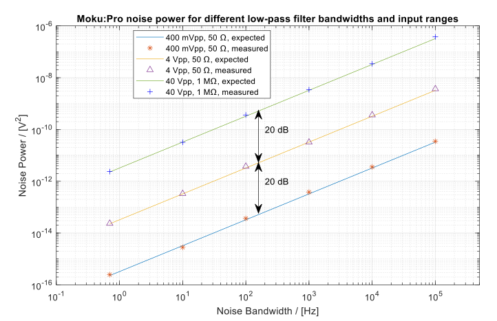
Figure 11: Noise power of the captured data under various lowpass filter corner frequencies and input ranges. The 20 dB input attenuations resulted in 20 dB increases in the equivalent noise levels.
In Figure 12, the noise ASD was calculated from the collected data. It’s notable that the overall shape of the ASD remains relatively consistent across different settings. The primary distinction lies in the overall noise level. For the maximum dynamic range, the noise floor of the 40 Vpp range increased by around 40 dB compared to the 400 mVpp range, attributed to the adjustment of the input attenuator from 0 dB to 40 dB.
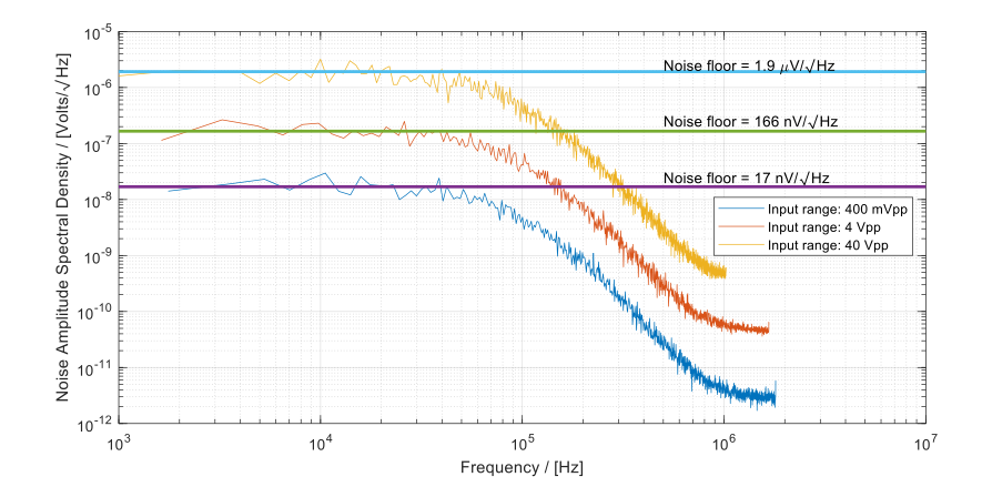
Figure 12: ASD of the noise data captured under different input ranges, with the lowpass filter frequency set to 100 kHz. The ASD between adjacent noise levels is approximately 10 times apart due to 20 dB attenuations.
Calculating SNR
As illustrated in the preceding sections, the noise power is directly correlated to the noise bandwidth. When dealing with a measured signal that is either a DC signal or a single-tone signal, the SNR can theoretically be enhanced to an infinitely high value. Real, measured SNR values will be presented in this section.
The SNR of the measured signal from the Lock-in Amplifier can be determined using Eq 5.1:
\(SNR = \frac{P_{signal}}{P_{noise}} = \frac{P_{signal}}{\int_{0}^{f_{lowpass}} S(f) \, df} \approx \frac{P_{signal}}{N_0\cdot f_{lowpass}}, (5.1) \)
assume S(f) is a flat noise floor→S(f)= N_0
Typically, the signal power, Psignal, is influenced by other components in the system, such as the photodetector or laser power. From this equation, it becomes evident that the SNR of the measured signal is inversely correlated with the lowpass filter corner frequency, assuming the noise PSD, S(f), remains constant.
To validate this theory, a test was devised where data was collected for various input ranges and lowpass filter bandwidths. The input signal was generated using a 10 MHz 100 µVpp single-tone signal generator with a 50 Ω source impedance. Subsequently, the single-tone signal was demodulated at the signal frequency 10 MHz to determine the input signal level. The corner frequency of the lowpass filter in the Lock-in Amplifier was then adjusted to several different values, and the SNR was calculated by dividing the square of the DC value by the variance of the demodulated signal. This approach was chosen because the DC level represents the signal, while the variance represents the noise power.
The results indicate that the measured SNR aligns with the expectation. It’s noteworthy that the SNR difference between the 4 Vpp and 40 Vpp settings is 14 dB instead of 20 dB, attributed to the configuration of the input impedance as 1 MΩ. A 1 MΩ load absorbs twice the voltage of a 50 Ω source port, resulting in a signal power four times (6 dB) that of the 50 Ω impedance.
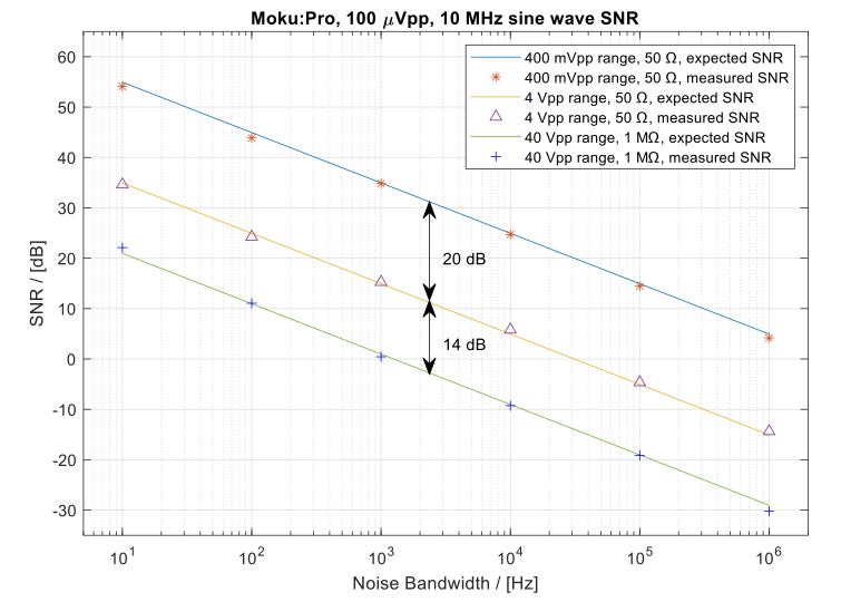
Figure 13: Measured and expected SNRs for various input ranges and noise bandwidths. The SNR scales proportionally to the expanded input range. The 14 dB SNR difference between the 4 Vpp and 40 Vpp ranges is attributed to the 1 MΩ input impedance. The absorption of twice the voltage results in a level that is four times higher (6 dB higher than 50 Ω ).
Discussion
In this section, various considerations will be explored, including the limitations of increasing the SNR by constraining the signal bandwidth and identifying suitable applications for bandwidth limitation.
When seeking to enhance the SNR of a measured signal, certain limitations should be acknowledged. A key constraint is the minimum bandwidth required by the signal, such as when analyzing phase or frequency shifts in a demodulated signal using a lock-in amplifier. In these scenarios, the lowpass filter bandwidth must exceed the frequency deviation or the rate of phase change. As a result, the lowpass filter bandwidth cannot be reduced indefinitely, which places an upper limit on the achievable SNR improvement. Therefore, limiting noise bandwidth reaches its maximum effectiveness when the expected signal is a DC signal or changes slowly over time.
To achieve the best possible SNR, the input range should be set to the minimum level that doesn’t clip the input signal. As illustrated in Figure 12, increasing input attenuation can raise the equivalent noise floor. Therefore, selecting a small input range is crucial when dealing with small signals to preserve a high SNR in the measured results.
Summary
This application note reviews the significance of the noise floor in both the time and frequency domains, and introduces methodologies to achieve a minimized noise in the measured signal. The noise floor not only conveys valuable information about the time-domain statistical noise distribution but also provides insights into the distribution of noise power across different frequency ranges. This becomes a valuable tool for users to predict the SNR and understand the optimal modulation frequency in practical experiments.
An effective method for enhancing SNR is to reduce the noise bandwidth in the experiment, which can be achieved through signal decimation or lowpass filtering to narrow the signal bandwidth. The application note also highlights optimal scenarios for implementing the noise bandwidth reduction method, identifying slow-changing experiments as particularly suitable for improving SNR by limiting the noise bandwidth.
Additionally, when comparing the noise performance between devices, it is crucial to also consider their dynamic ranges rather than just the absolute noise floor. Generally, a small input range corresponds to a low noise floor. However, if the signal amplitude exceeds this small range, it can result in degraded noise performance by switching to a larger range. Therefore, one should always ensure that the input ranges are comparable when evaluating the noise floors of two devices.
Questions?
Get answers to FAQs in our Knowledge Base
If you have a question about a device feature or instrument function, check out our extensive Knowledge Base to find the answers you’re looking for. You can also quickly see popular articles and refine your search by product or topic.
Join our User Forum to stay connected
Want to request a new feature? Have a support tip to share? From use case examples to new feature announcements and more, the User Forum is your one-stop shop for product updates, as well as connection to Liquid Instruments and our global user community.