Dr Ji-Zhe Zhang from the Institute of Chemistry, Chinese Academy of Sciences, has proposed a novel reconfigurable solution for integrated optical chips. The team successfully developed an organic photoactuator with programmable motion trajectories. Driven by low-power lasers, this actuator enables straight-line movement, turning, crossing waveguides, and manipulating microstructures on optical chips. Based on this, the team achieved the first dynamic, semi-permanent, and precise control of the resonance frequency of micro-ring resonators on a photonic chip. The research findings were recently published in the journal Nature Communications.
In their research they used Moku:Lab, an FPGA-based device from Liquid Instruments that delivers a reconfigurable suite of test and measurement instruments for fast, flexible signal processing and analysis. Leveraging the PID Controller, the group could stabilize their laser power over long periods of time, enabling them to verify the repeatability of their measurements.
The challenge
Rewritable photonic integrated circuits are core components for future adaptive optical computing, quantum information processing, and intelligent sensing systems. The post-assembly and dynamic reconfiguration capabilities of their micro-nano structures pose significant challenges in this field. Traditional device control methods often require a con-tinuous power supply. Existing micro-manipulation techniques, such as optical tweezers, necessitate operation in liquid environments, while near-field probes risk damaging devices. Neither approach adequately meets the demands for on-chip, non-liquid, non-destructive, and low-power manipulation.
The solution
Recent advances [1,2] in light-driven organic materials have established a basis for micro-actuators that convert localized optical excitation into mechanical motion. The research team utilized indigo-based donor-acceptor molecules to fabricate organic microcrystalline photomechanical actuators. When driven by 405 nm laser light, these actuators achieve precise motion on various photonic chip substrates including silicon, silicon nitride, sapphire, and lithium niobate. By developing a custom scanning mirror control system, the present work demonstrates a fully programmable, optically driven organic nano-step actuator. It achieved single-step positioning accuracy of 30 nm and multi-degree-of-freedom capabilities including forward/reverse motion and lateral steering. Furthermore, it enabled precise positioning of 22-micrometer-diameter silica microspheres, showcasing robust micro-nano manipulation performance.
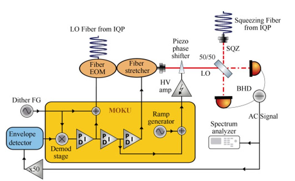
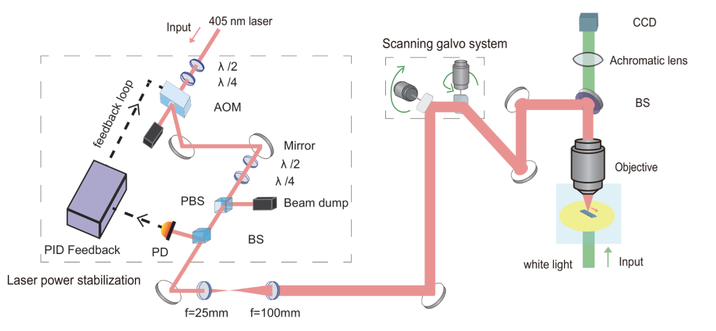
Reliable operation of the actuator depends critically upon stable optical excitation and ac-curate motion monitoring. The experimental setup is divided into two modules: a laser scanning module and an imaging module, as seen in Figure 1.
In the laser scanning module, the actuation beam is stabilized by an acousto-optic modula-tor (AOM) driven by an RF source. The transmitted beam is monitored by a photodiode, and a feedback loop implemented on the Moku:Lab PID Controller continuously adjusts the AOM modulation power. The PID Controller dynamically adjusts the RF power applied to the AOM by comparing the measured value from the branch optical detector with the setpoint and stabilizes the laser power. After a series of feedback adjustments, the relative deviation between the laser power in the main optical path and the setpoint is maintained at approximately 0.5%, meeting the experimental requirements for laser power stability in the main optical path.
The imaging module provides high-resolution characterization of actuator dynamics. A CCD camera combined with a high-numerical-aperture objective lens acquires images of the actuator trajectory. These images are processed by an automated image-analysis system, which determines displacement and with high precision, enabling quantitative evaluation of motion.
The result
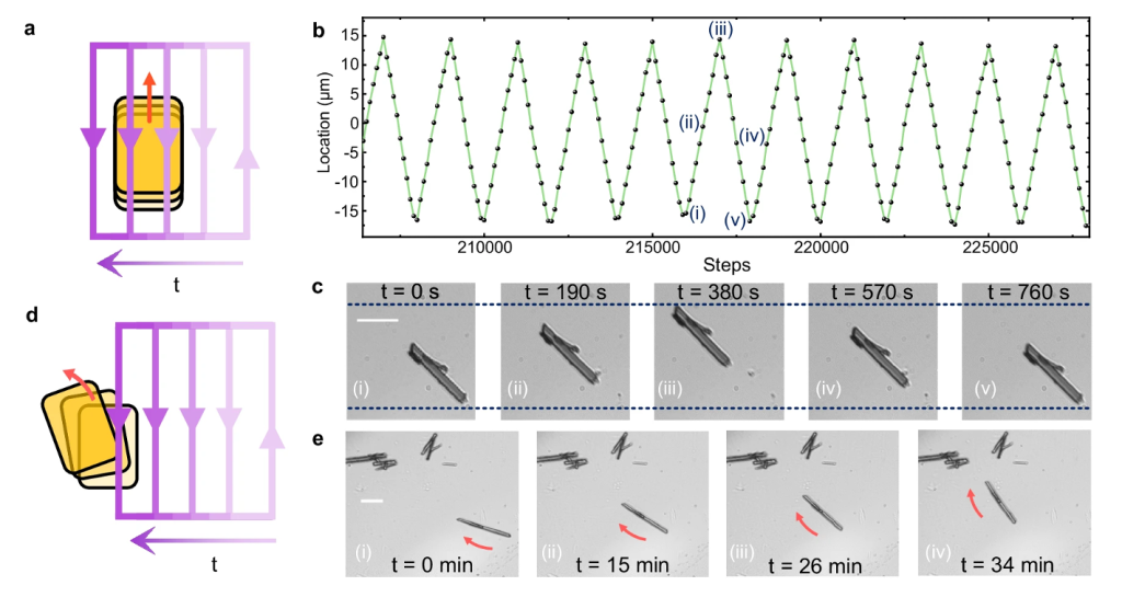
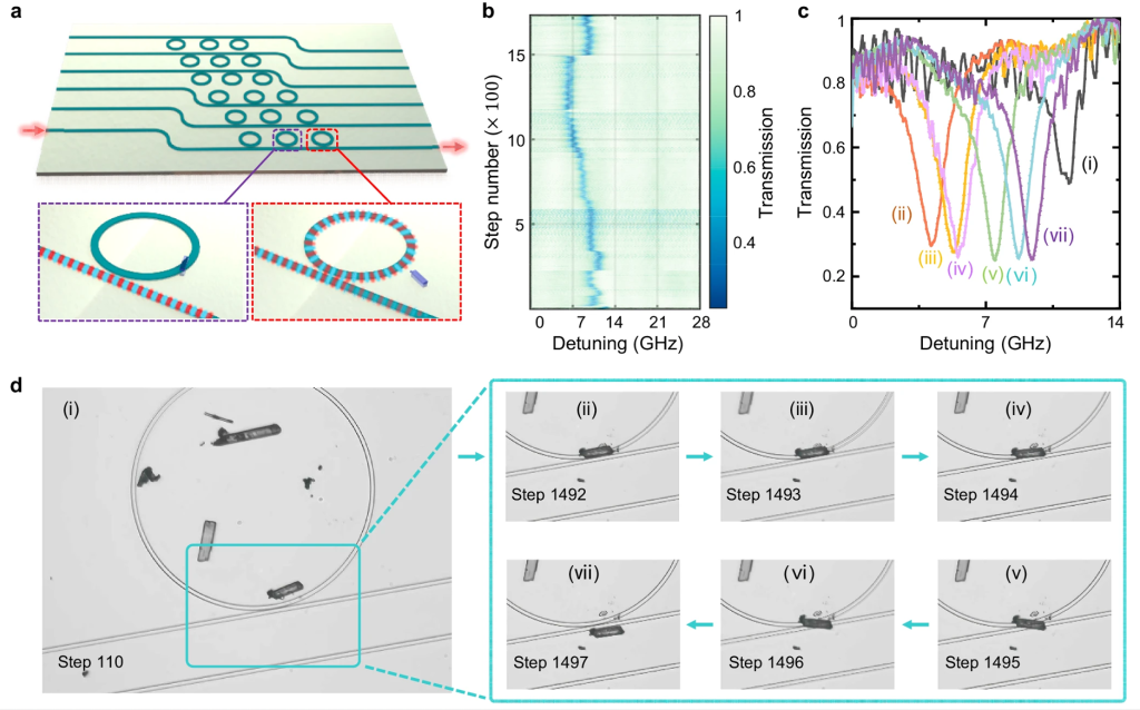
Figure 2 demonstrates the programmable motion control of the organic nano-step actuator through tailored laser scanning trajectories. Straight displacement is achieved by scanning across the full actuator width, as shown in Figure 2a, with the direction of motion opposite to that of the scanning laser spots; reversing the scan direction reverses the actuator’s movement. The long-term stability of this behavior is confirmed in Figure 2b, which shows a displacement trace obtained by tracking the actuator position after every 100 scans, with 2000 steps accumulated per cycle. Corresponding CCD snapshots in Figure 2c capture one complete forward–reverse sequence, yielding a displacement of 30.2 ± 1.1 µm per 1000 steps, equivalent to a step size of approximately 30 nm. Beyond straight motion, photomechanical actuators operate on the principle that a scanned laser beam deforms the underlying lattice. This deformation, in turn, causes the actuator’s position to change. If the laser beam only covers one side of the actuator, the distance traveled by that side during scanning will be greater than the other side, causing the actuator to turn.
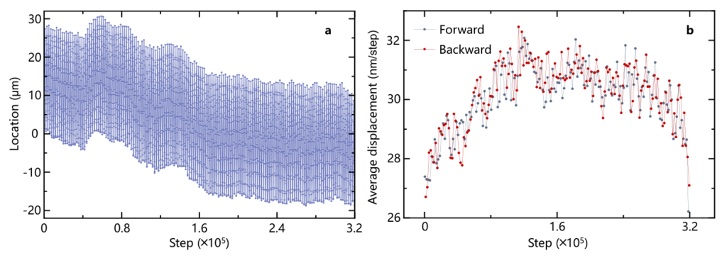
The stabilized system supports long-term operation with high repeatability, as shown in Figure 3. Continuous actuation was carried out over 3.2 × 10^5 steps, with images record-ed every 100 steps to monitor displacement. Across 1000-step intervals, the actuator exhibited average displacements of 29.84 ± 1.21 nm in the forward direction and 30.01 ± 1.31 nm in the backward direction per step. After the initial cleaning of surface contaminants through repeated actuator motion, the displacement further stabilized during the subsequent 1.6 × 10^5 steps, reaching 30.31 ± 0.88 nm (forward) and 30.37 ± 0.88 nm (backward). These results demonstrate excellent reproducibility and stability of the actuator under extended operation.
The capability of the actuator to overcome structural barriers is demonstrated on integrated lithium niobate (LN) photonic circuits fabricated on sapphire substrates, where it successfully traverses wedge-shaped LN waveguides with a thickness of 220 nm and engages with a microring resonator. When positioned across the optical path of the resnator, the actuator induces a resonance shift of 5.2 GHz. Crucially, the quality factor of the microring remains stable, with linewidth variations below 16%, and fully recovers to its initial value after the actuator is removed. These results provide a novel approach for achieving non-volatile reversible, low-loss, and non-destructive dynamic control of integrated photonic circuits.
The organic nano-step actuator offers advantages such as low power consumption, non-invasiveness, and strong compatibility with existing photonic technology. They can be used not only for post-tuning and reconstruction of photonic devices but also provide a universal technical platform for the precise positioning and assembly of functional materials on-chip, such as gain media, nonlinear crystals, and phase-change materials. This approach provides a practical and reversible complement to top-down fabrication, advancing technological fields including adaptive integrated photonic circuits, organic-inorganic hybrid optoelectronic integrated systems, and nanorobotics.
Dr. Jizhe Zhang remarked, “Moku has indeed become an indispensable tool in precision measurement experiments. Its outstanding performance, combined with an interface that is simple to use yet far from simplistic, was the defining characteristic that impressed us greatly when the product first appeared. I hope Moku continues to maintain this distinctive quality.”
References
[1] Gong, Y. et al. Light-driven crawling of molecular crystals by phase-dependent transient elastic lattice deformation. Angew. Chem. Int. Ed. 59, 10337–10342 (2020).
[2] Zhang, Y. et al. Light-driven continuous twist movements of microribbons. Small 15, 1804102 (2019).
[3] Zhang, JZ. et al. Optically-driven organic nano-step actuator for reconfigurable photonic circuits. Nat Commun 16, 8213 (2025).