
This white paper outlines how to use IP cores in Moku Cloud Compile, including eight precompiled IP cores for common signal processing functions and custom AMD Vivado IP core integration. Each core is described with usage examples and test setups using Moku hardware. The document also guides users through uploading custom IPs.
Introduction
Moku Cloud Compile is a powerful tool available on Moku devices. Moku FPGA-based test and measurement devices allow users to deploy custom VHDL and Verilog code to the hardware. With Moku Cloud Compile, you can extend and customize instrument functionality by integrating your own designs with existing instruments to create new capabilities made possible by Moku’s unique Instrument-on-Chip architecture.
Moku Cloud Compile offers eight precompiled IP cores optimized for arithmetic, filtering, waveform generation, and correlation analysis, compatible with all Moku devices. These cores are ready to instantiate and simplify common digital signal processing tasks. Users can also import their own IP cores created in AMD Vivado by uploading .xci files, enabling seamless integration of custom hardware blocks into Moku Cloud Compile designs.
This document outlines the in/out ports, functionality, and example usage of each IP core, and provides guidance on building and testing custom designs using Multi-Instrument Mode. Together, these features make Moku Cloud Compile a more powerful platform for both rapid prototyping and advanced signal processing applications.
Eight precompiled IP cores
This section describes the eight precompiled IP cores listed in Table 1, detailing their input and output port specifications and functionality. Example use cases are provided for each core. Owing to their native integration within the Moku Cloud Compile backend, these IP cores can be instantiated directly within user designs, thereby streamlining the development process and reducing implementation overhead.
Table 1: The names and descriptions of the eight precompiled IP cores.
| No. | IP core name | Description |
| 1 | AddSubtract_16 | Dynamically reconfigurable adder/subtractor module. |
| 2 | CIC_Dec_3Ordx8 | Cascaded Integrator-Comb (CIC) decimator with a decimation factor of 8 and filter order of 3. |
| 3 | Cordic_Translate_16 | Converter that transforms 16-bit real and imaginary inputs into amplitude and phase outputs. |
| 4 | Counter_32 | 32-bit counter supporting up/down counting with synchronous clear functionality. |
| 5 | SineGen_48 | Sine and cosine waveform generator with a 48-bit frequency step resolution. |
| 6 | FIR_Filter_7coef | Full-rate FIR low-pass filter with fixed coefficients. |
| 7 | FFT_1024 | 1,024-point fast Fourier transform (FFT) block with selectable forward or inverse transform. |
| 8 | FFT_65536 | 65,536-point fast Fourier transform (FFT) block with selectable forward or inverse transform and configurable output scaling. |
1. AddSubtract_16
The AddSubtract_16 module implements a dynamically configurable arithmetic unit capable of performing either addition or subtraction on two signed 16-bit inputs. Its operation is governed by the following logic:
$latex S =left{ begin{array}{rl}
A + B text{(add: HIGH)} \
A – B text{(add: LOW)}
end{array} right.$
The input and output ports of the AddSubtract_16 core are detailed in Table 2. Both input buses (A and B) and the output (S) are treated as signed 16-bit integers (int16). The arithmetic operation is controlled by the add signal, while the ce (clock enable) signal enables or disables the clock of the module. When ce is held high, the module remains continuously active.
Table 2: Port definitions for the AddSubtract_16 module, detailing its input and output signal interfaces.
|
Name |
Direction | Description |
| A[15:0] | Input | Input A bus. |
| B[15:0] | Input | Input B bus. |
| clk | Input | Clock signal, rising edge. |
| add | Input | Controls the operation performed by AddSubtract_16.
(HIGH = Addition, LOW=subtraction) |
| ce | Input | Active-HIGH clock enable. Set to constant high. |
| S[15:0] | Output | Output bus. |
Code 1 provides a VHDL example demonstrating how to instantiate the module and control using the 0th bit (least significant bit, LSB) of Control0. The Multi-Instrument Mode configuration is illustrated in Figure 1. Test results shown in Figures 2 and 3, conducted using Moku hardware, confirm correct subtraction and addition behavior under varying signal conditions.
Code 1: The VHDL example demonstrates the instantiation of the AddSubtract_16 module, where OutputA represents the result of either InputA + InputB or InputA – InputB, depending on the state of the LSB of the Control0 register.
LIBRARY ieee;

ARCHITECTURE Behavioral OF CustomWrapper IS

	SIGNAL s_temp : STD_LOGIC_VECTOR(15 DOWNTO 0);

BEGIN

	AddSubtract : AddSubtract_16
	PORT MAP(
		A => STD_LOGIC_VECTOR(InputA),
		B => STD_LOGIC_VECTOR(InputB),
		clk => clk,
		-- use Control0's 0th bit to control the operation
		add => Control0(0),
		-- constant high clock enable
		ce => '1',
		S => s_temp
	);

	OutputA <= signed(s_temp);

END ARCHITECTURE;
Figure 1: Test configuration for the AddSubtract_16 using Multi-Instrument Mode. In this setup, InputA and InputB of Moku Cloud Compile are internally routed from the outputs of the Moku Oscilloscope, while the processed output from Moku Cloud Compile is fed back into the Oscilloscope.
As shown in Figure 2, the two-channel embedded waveform generators in the Moku Oscilloscope are configured to produce a 5 kHz, 500 mV sine wave and a 100 Hz, 5 Vpp ramp signal with 90% symmetry. With the LSB of Control0 set to 0, Moku Cloud Compile operates in subtraction mode. The observed output on the Moku Oscilloscope confirms the expected subtractor behavior. Subsequently, in Figure 3, the LSB of Control0 is set to 1, configuring Moku Cloud Compile to perform addition. The resulting output confirms the expected adder functionality.
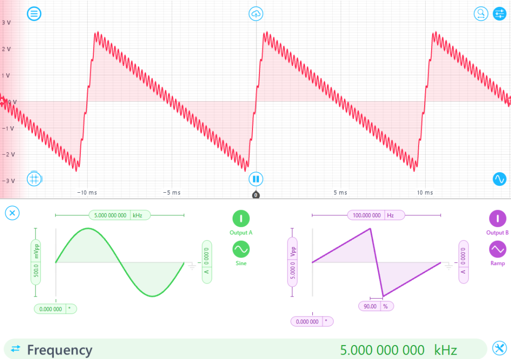
Figure 2: Moku Cloud Compile outputs subtracted results using two input signals: a 500 mVpp, 5 kHz sine wave and a 5 Vpp, 100 Hz ramp wave. With Control0(0) set to 0, the system is configured to operate in subtraction mode.
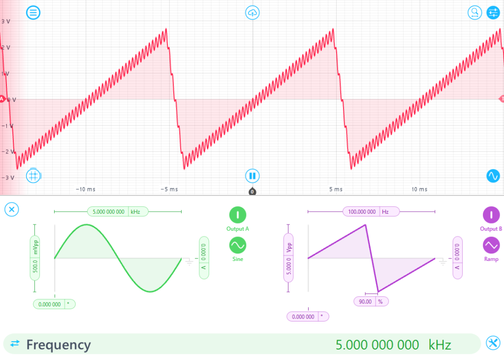
Figure 3: Moku Cloud Compile output in response to a 500 mVpp 5 kHz sine wave and a 5 Vpp, 100 Hz ramp wave. With Control0(0) set to 1, the system is configured for addition mode.
It is important to note that the AddSubtract_16 module does not include a carry-out mechanism and may therefore experience overflow during arithmetic operations. Specifically, if the sum of Input A + Input B exceeds the signed 16-bit range \([-2^{15}, 2^{15}]\) , the output may exhibit a sign inversion due to overflow.
A common method for detecting potential overflow involves monitoring the most significant bit (MSB) of the operands and the result. No overflow occurs if the inputs have opposite signs. However, if both inputs share the same sign and the output sign differs, this typically indicates an overflow condition. While this paper acknowledges the issue, a detailed discussion of overflow detection and mitigation techniques is beyond its current scope.
The input sources are configured as a 5 Vpp sine wave and a 5 V DC signal. Theoretically, this combination should produce an output waveform ranging from 2.5 V to 7.5 V. However, the Moku:Go hardware is limited to a ±5 V input/output range (10 Vpp). As a result, any portion of the output that exceeds this range will experience a sign inversion due to overflow. This behavior is illustrated in Figure 4, where the portions of the waveform that should lie between 5 V and 7.5 V are instead wrapped around and appear between −2.5 V and −5 V.
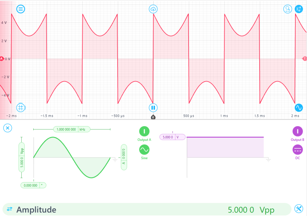
Figure 4: The addition of a 5 Vpp, 1 kHz sine wave and a 5 V DC offset results in observable overflow, as the signal exceeds the ±5 V input range of the Moku:Go device. With Control0(0) set to 1, the system operates in addition mode, and a sign inversion in the output confirms the occurrence of overflow.
2. CIC_Dec_3Ordx8
The CIC_Dec_3Ordx8 module implements a 3rd-order Cascaded Integrator-Comb (CIC) decimation filter with a fixed decimation rate of 8. CIC filters are widely used in multi-rate systems where a high sampling rate needs to be reduced. The architecture relies solely on adders, subtractors, and delays, making it ideal for hardware-efficient downsampling applications such as digital receivers and lock-in amplifiers.
The input and output ports of the module are summarized in Table 3, while the implementation details such as latency and filter order are provided in Table 4. The module accepts 16-bit signed input samples and produces 25-bit signed output samples. The input interface provides handshake signals (tvalid, tready) for both input and output channels. The filter updates its output only when valid input is received, and the core is ready.
Table 3: Port descriptions for the CIC_Dec_3Ordx8 IP core.
| Name | Direction | Description |
| aclk | Input | Clock signal, rising edge. |
| s_axis_data_tdata [15:0] | Input | TDATA for the Data Input Channel. Carries the unprocessed sample data. |
| s_axis_data_tvalid | Input | TVALID for the Data Input Channel. Used by the external block to signal that it is able to provide data. |
| s_axis_data_tready | Output | TREADY for the Data Input Channel. Used by the CIC decimator to signal that it is ready to accept data. |
| m_axis_data_tdata [24:0] | Output | TDATA for the Data Output Channel. Carries the processed sample data. |
| m_axis_data_tvalid | Output |
TVALID for the Data Output Channel. Asserted by the CIC decimator to signal that it is able to provide sample data. |
Table 4: Configuration parameters of the CIC_Dec_3Ordx8 IP core.
|
Component Name |
CIC_Dec_3Ordx8 |
| Filter Type | Decimation |
| Number of Stages | 3 |
| Differential Delay | 1 |
| Rate Supported | 8 |
| Input Sample Frequency (MSa/s) | 31.25 |
| Clock Frequency (MHz) | 31.25 |
| Input Data Width | 16 |
| Output Data Width | 25 |
| Latency |
15 |
In the provided VHDL example shown in Code 2, input data is written only when the core is ready (s_axis_data_tready is high), and output is captured only when valid data is available (m_axis_data_tvalid is high). The output is scaled by truncating to the most significant 16 bits to maintain consistency with the input dynamic range. It is important to note that the valid signal must be asserted, and the output should be updated only when this signal is high. Otherwise, the output may exhibit pulsed or intermittent behavior rather than a continuous stream. This occurs because the CIC_Dec_3Ordx8 generates a single valid output sample for every eight clock cycles, in accordance with its decimation factor.
Code 2: VHDL example demonstrating the instantiation of a CIC decimator with an 8x decimation factor. The signal OutputA represents the downsampled version of the signal InputA.
LIBRARY ieee;

ARCHITECTURE Behavioral OF CustomWrapper IS

	SIGNAL s_axis_data_tready : STD_LOGIC;
	SIGNAL s_axis_data_tdata : STD_LOGIC_VECTOR(15 DOWNTO 0);

	SIGNAL m_axis_data_tvalid : STD_LOGIC;
	SIGNAL m_axis_data_tdata : STD_LOGIC_VECTOR(31 DOWNTO 0);

BEGIN

	Decimator : CIC_Dec_3Ordx8
	PORT MAP(
		aclk => clk,
		s_axis_data_tdata => s_axis_data_tdata,
		s_axis_data_tvalid => '1', -- always output
		s_axis_data_tready => s_axis_data_tready,
		m_axis_data_tdata => m_axis_data_tdata,
		m_axis_data_tvalid => m_axis_data_tvalid
	);

	PROCESS (clk)
	BEGIN
		IF rising_edge(clk) THEN

			-- update input data when CIC is ready
			IF s_axis_data_tready THEN
				s_axis_data_tdata <= STD_LOGIC_VECTOR(InputA);
			ELSE
				s_axis_data_tdata <= (OTHERS => '0');
			END IF;

			-- update Output only when data is valid
			IF m_axis_data_tvalid THEN
				-- Scale data correctly
				OutputA <= signed(m_axis_data_tdata(24 DOWNTO 9));
			END IF;

		END IF;
	END PROCESS;

END ARCHITECTURE;
A Multi-Instrument Mode test setup uses the Moku Frequency Response Analyzer to evaluate the filter’s frequency response is shown in Figure 5. The frequency response of the CIC filter is of particular interest, as it characterizes the attenuation of out-of-band signals and reflects its effectiveness in suppressing aliasing noise during decimation. Measured results in Figure 6 and Figure 7 show good alignment with theoretical expectations, accounting for expected discrepancies due to decimation and interpolation artifacts.
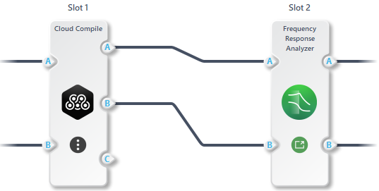
Figure 5: Multi-Instrument Mode test configuration in which the Moku Cloud Compile output is analyzed using the Moku Frequency Response Analyzer.
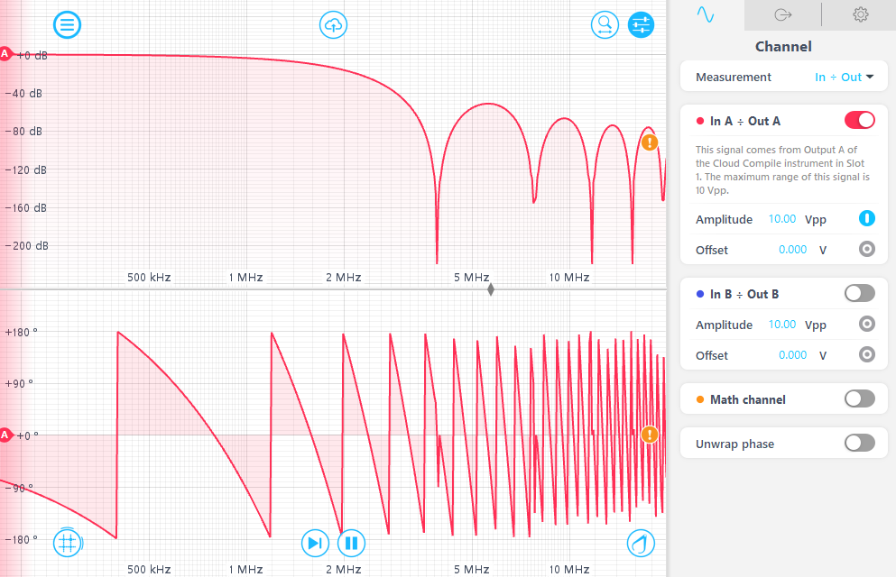
Figure 6: Frequency response of the CIC_Dec_3Ordx8 IP core as obtained using the Moku Frequency Response Analyzer.
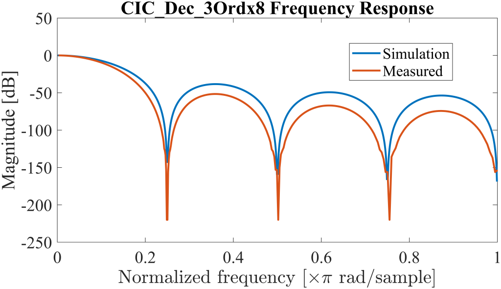
Figure 7: Comparison between the simulated and implemented responses of the CIC_Dec_3Ordx8.
3. Cordic_Translate_16
The CORDIC core implements the Coordinate Rotation Digital Computer (CORDIC) algorithm, an iterative method used to compute trigonometric functions and, more generally, to solve equations involving hyperbolic and square root operations. The input and output port descriptions are provided in Table 5. This Cordic_Translate_16 core transforms input signals from their Cartesian representation (real and imaginary components) into their corresponding polar form (amplitude and phase). The total computational latency of the module is 20 clock cycles.
Table 5: Port definitions of Cordic_Translate_16 IP core.
|
Name |
Direction | Description |
| aclk | Input | Clock. Active rising edge. |
| s_axis_cartesian_tvalid | Input | Handshake signal for channel S_AXIS_CARTESIAN. |
| s_axis_cartesian_tdata [31:0] | Input | Depending on Functional Configuration, this port has one or two subfields.
X_IN and Y_IN, X_IN is [15:0] and Y_IN is [31:16]. These are the Cartesian operands. Each subfield is 16-bit wide. X_IN and Y_IN both have 14 fractional bits and 2 integer bits. |
| m_axis_dout_tvalid | Output | Handshake signal for output channel. |
| m_axis_dout_tdata [31:0] | Output |
Depending on Functional Configuration this port contains the following subfields. AMPLITUDE_OUT, PHASE_OUT. AMPLITUDE_OUT is [15:0] and PHASE_OUT is [31:16]. Each subfield is 16-bit wide. AMPLITUDE_OUT has 14 fractional bits and 2 integer bits. PHASE_OUT has 13 fractional bits and 3 integer bits with a unit of radians. |
The Cordic_Translate_16 IP core can be instantiated using Code 3, which converts the imaginary (InputA) and real (InputB) components of a signal into their corresponding amplitude (OutputA) and phase angle (OutputB).
Code 3: VHDL implementation example demonstrating the instantiation of a Cordic_Translate_16 IP core.
LIBRARY ieee;

ARCHITECTURE Behavioral OF CustomWrapper IS

	SIGNAL m_axis_dout_tvalid : STD_LOGIC;
	SIGNAL tdata_temp : signed(31 DOWNTO 0);

BEGIN
	Cordic : Cordic_Translate_16
	PORT MAP(
		aclk => clk,
		-- input is always valid
		s_axis_cartesian_tvalid => '1',
		-- InputA : imaginary part
		-- InputB : real part
		s_axis_cartesian_tdata => STD_LOGIC_VECTOR(InputA & InputB),
		m_axis_dout_tvalid => m_axis_dout_tvalid,
		m_axis_dout_tdata => tdata_temp
	);

	PROCESS (clk)
	BEGIN
		IF rising_edge(clk) THEN

			IF m_axis_dout_tvalid THEN
				OutputA <= signed(tdata_temp(15 DOWNTO 0));
				OutputB <= signed(tdata_temp(31 DOWNTO 16));
			END IF;

		END IF;
	END PROCESS;

END ARCHITECTURE;
The instantiated Cordic_Translate_16 is tested using the Multi-Instrument Mode setup shown in Figure 8. Moku Cloud Compile InputA (imaginary) and InputB (real) are internally routed from the Moku Oscilloscope outputs to Moku Cloud Compile, which computes the corresponding amplitude and phase outputs. These Moku Cloud Compile outputs are then routed back to the Oscilloscope for visualization and analysis.
The results are shown in Figure 9. The blue trace reaches a peak value of 3.9288 V, corresponding to approximately 3.1415 radians. Since the phase output is represented with 13 fractional bits, the resolution is 2^13 LSBs/rad. To convert the digital values into physical units, the digital resolution of Moku Cloud Compile must be determined and can be found here. Given a digital resolution of 6550.4 LSBs/V on Moku:Go, the radian value is calculated as:
\(frac{text{3.9288 V} times text{6550.4 LSBs/V}}{2^{13} text{LSBs/rad}}=text{3.1415 rad}\)
Furthermore, the amplitude output increases in magnitude by a factor of approximately 1.1644 due to the accumulation of scaling effects introduced during the 20 iterations performed by the Cordic_Translate_16.

Figure 8: Multi-Instrument Mode test setup for testing Cordic_Translate_16 IP core.
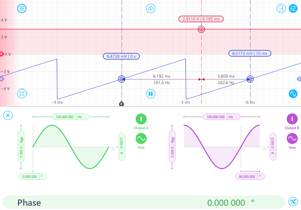
Figure 9: Two output channels are configured with 100 Hz sine waves at 5 Vpp offset by a 90° phase shift to emulate a continuously rotating complex vector. InputA (red trace) represents the amplitude, while InputB (blue trace) corresponds to the phase. As expected, the amplitude remains constant while the phase increases linearly over time, wrapping every 2𝜋 radians.
4. Counter_32
The Counter_32 IP core offers counter implementations utilizing lookup tables (LUTs) and single DSP slices. The input and output port functions are described in Table 6. It supports up/down counting modes with output widths of 32 bits. The counter increments by one on each clock cycle and can be synchronously cleared by pulling the SCLR signal high.
Table 6: Port definitions of Counter_32.
| Name | Direction | Description |
| CLK | Input | Rising edge clock signal. |
| SCLR | Input | Synchronous Clear: forces the output to a low state when driven high. |
| UP | Input | Controls the count direction on an up/down counter. Counts up when high, down when low. |
| Q [31:0] | Output |
Counter output. 32-bit wide. |
The example in Code 4 implements two Counter_32 functions: one configured for bidirectional counting to generate a triangular waveform, and the other for unidirectional counting to produce a sawtooth waveform. Only the least significant 16 bits of the counters are connected to the outputs, as the design operates within a range below 65,536.
Code 4: VHDL example instantiating two Counter_32 for triangular and sawtooth waveforms.
LIBRARY ieee;

ARCHITECTURE Behavioural OF CustomWrapper IS

	SIGNAL sclr_triangular : STD_LOGIC;
	SIGNAL sclr_sawtooth : STD_LOGIC;

	SIGNAL up_triangular : STD_LOGIC;
	SIGNAL up_sawtooth : STD_LOGIC;

	SIGNAL q_triangular : STD_LOGIC_VECTOR(31 DOWNTO 0);
	SIGNAL q_sawtooth : STD_LOGIC_VECTOR(31 DOWNTO 0);

BEGIN

	-- Triangular wave
	Triangular : Counter_32
	PORT MAP(
		clk => clk,
		-- synchronous clear
		sclr => sclr_triangular,
		up => up_triangular,
		q => q_triangular
	);
	OutputA <= signed(q_triangular(15 DOWNTO 0));

	-- Triangular counter configuration
	PROCESS (clk) IS
	BEGIN
		IF rising_edge(clk) THEN
			-- reset
			IF Control0(0) = '1' THEN
				sclr_triangular <= '1';
				up_triangular <= '1';
			ELSE
				-- don't clear
				sclr_triangular <= '0';
				-- Control1: counter limit
				IF q_triangular = Control1 THEN
					-- count down
					up_triangular <= '0';
				ELSIF q_triangular = x"00000000" THEN
					-- count up
					up_triangular <= '1';
				ELSE
					-- hold
					up_triangular <= up_triangular; END IF; END IF; END IF; END PROCESS; Sawtooth : Counter_32 PORT MAP( clk => clk,
		sclr => sclr_sawtooth, -- synchronous clear
		up => up_sawtooth,
		q => q_sawtooth
	);
	OutputB <= signed(q_sawtooth(15 DOWNTO 0));

	-- Sawtooth counter configuration
	PROCESS (clk) IS
	BEGIN
		IF rising_edge(clk) THEN
			-- reset
			IF Control0(0) = '1' THEN
				sclr_sawtooth <= '1';
				up_sawtooth <= '1';
			ELSE
				-- always count up
				up_sawtooth <= '1';
				-- Control2 : counter limit
				IF q_sawtooth = Control2 THEN
					-- clear
					sclr_sawtooth <= '1';
				ELSE
					-- continue counting
					sclr_sawtooth <= '0';
				END IF;
			END IF;
		END IF;
	END PROCESS;

END ARCHITECTURE;
The Multi-Instrument Mode configuration is illustrated in Figure 10. The Moku Oscilloscope is employed to visualize the waveforms generated by two Counter_32 modules. Both counters are configured with control values of 6,550 through Control1 and Control2, resulting in a peak output of approximately 1 V, based on the Moku:Go digital resolution of 6550.4 LSBs/V. The LSB of Control0 functions as a reset signal and must be set to high and back to low prior to operation. As expected, the sawtooth waveform has twice the frequency of the triangular waveform, since it counts only upward, while the triangular waveform alternates between upward and downward counting cycles.
The test results are presented in Figure 11. The red trace represents the triangular waveform, generated by alternating up and down counting. The blue trace corresponds to the sawtooth waveform, which increments continuously and resets upon reaching the configured limit of 6,550.
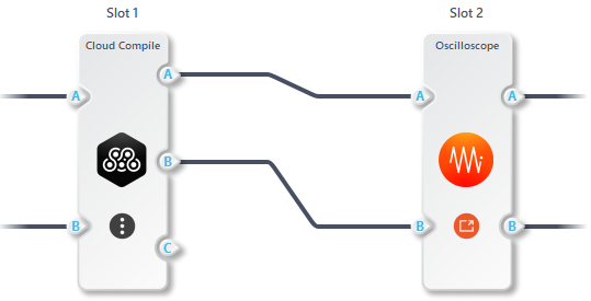
Figure 10: Multi-Instrument Mode configuration for testing Counter_32.
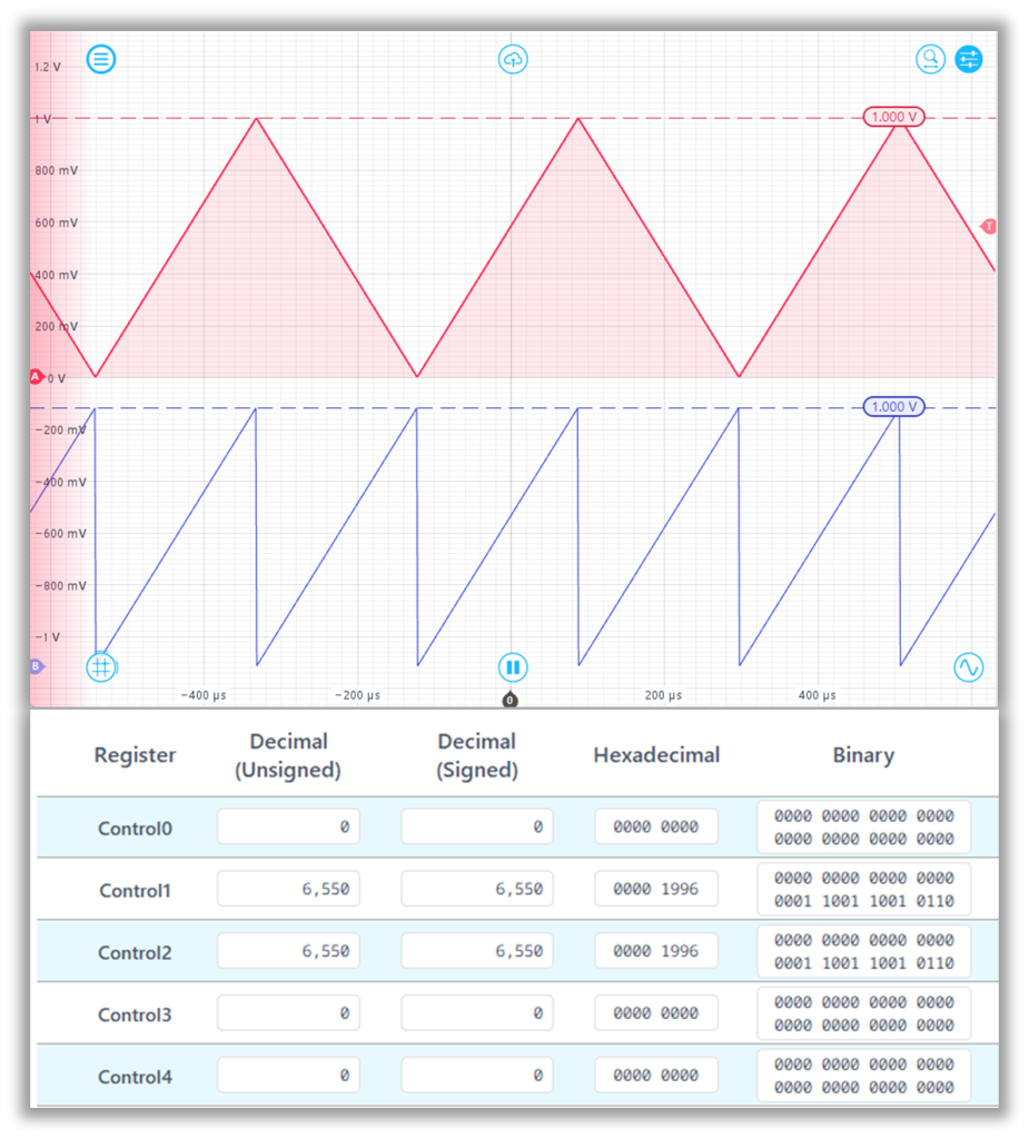
Figure 11: Configuration of Moku Cloud Compile control registers and corresponding outputs of the two Counter_32 modules.
5. SineGen_48
The SineGen_48 IP core generates high-resolution, low-distortion sine waveforms. Its input and output ports are detailed in Table 7. It accepts a 48-bit frequency step input and produces both 16-bit sine and cosine outputs through a 32-bit output port. This module serves as a sine waveform generator subblock suitable for a range of advanced applications, including phase-locked loops and simultaneous amplitude and frequency modulation (AM and FM).
Since the SineGen_48 IP core requires a 48-bit frequency step input, and Moku Cloud Compile control registers are limited to 32 bits, two registers must be combined to form the full 48-bit input. For example, in Code 5, the least significant 16 bits of Control2 are concatenated with the 32 bits of Control1 to construct the complete frequency control word. The generated output is divided into two 16-bit components, corresponding to the sine and cosine waveforms, which are routed to OutputA and OutputB, respectively. Additionally, the most significant 16 bits of the internal phase counter are directed to OutputC.
Code 5: VHDL instantiation example of SineGen_48.
LIBRARY ieee;

ARCHITECTURE Behavioural OF CustomWrapper IS

	SIGNAL m_axis_data_tvalid : STD_LOGIC;
	SIGNAL m_axis_phase_tvalid : STD_LOGIC;
	SIGNAL sine_temp : STD_LOGIC_VECTOR(31 DOWNTO 0);
	SIGNAL m_axis_phase_tdata : STD_LOGIC_VECTOR(47 DOWNTO 0);

BEGIN

	SineCosineGen : SineGen_48
	PORT MAP(
		aclk => clk,
		-- Use the 0th bit of Control0 to reset this module
		aresetn => NOT Control0(0),
		-- input signal is always available
		s_axis_config_tvalid => '1',
		-- 48-bit frequency step
		s_axis_config_tdata => Control2(15 DOWNTO 0) & Control1,

		m_axis_data_tvalid => m_axis_data_tvalid,
		m_axis_data_tdata => sine_temp,

		m_axis_phase_tvalid => m_axis_phase_tvalid,
		m_axis_phase_tdata => m_axis_phase_tdata -- 48-bit phase counter output
	);

	-- only output data when data is valid
	PROCESS (clk)
	BEGIN
		IF rising_edge(clk) THEN

			IF m_axis_data_tvalid THEN
				-- 32-bit, the most significant 16 bits are sine
				-- and the least significant 16 bits are cosine
				OutputA <= signed(sine_temp(15 DOWNTO 0));
				OutputB <= signed(sine_temp(31 DOWNTO 16));
			END IF;

			IF m_axis_phase_tvalid THEN
				OutputC <= signed(m_axis_phase_tdata(47 DOWNTO 32));
			END IF;

		END IF;
	END PROCESS;

END ARCHITECTURE;
The Multi-Instrument Mode configuration for testing the SineGen_48 IP core is shown in Figure 12. The frequency step is set to 3.125 kHz by configuring Control1 to 2,374,548,092 and Control2 to 6. The full 48-bit frequency control word is calculated as:
\(text{Frequency step} = text{Control 2} times 2^{32} + text{Control 1} = 2,814,749,767\)
And the frequency in the unit of Hz can be calculated as:
\(text{Frequency} = frac{text{clock rate}}{2^{48}}times [text{Control 2} times 2^{32} + text{Control 1}]\)
Given that the Moku:Go clock rate is 31.25 MHz, the output frequency becomes 3.125 kHz.
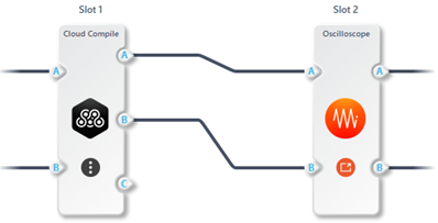
Figure 12: Multi-Instrument Mode configuration for testing SineGen_48 IP core.
Figure 13 displays the output of the SineGen_48 IP core, where Channel A (red) represents the cosine waveform and Channel B (blue) represents the sine waveform. The measured phase difference between the two signals is 90°, as expected. Additionally, Figure 14 illustrates the behavior of the phase counter routed to OutputC of Moku Cloud Compile. The output shows a continuously increasing ramp, confirming that the phase signal advances at the same frequency as the generated cosine waveform.
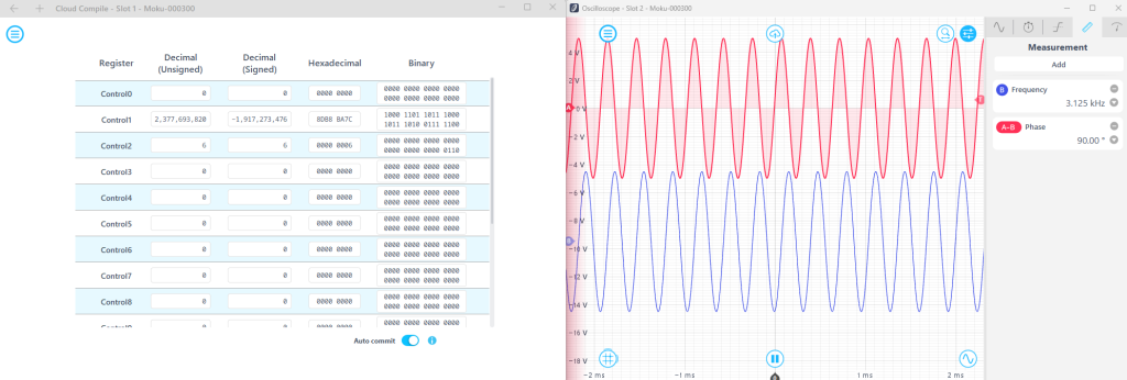
Figure 13: Sine and cosine waveforms visualized using the Moku Oscilloscope. Channel A (red) displays the cosine signal, while Channel B (blue) shows the sine signal. The frequency step is configured with Control1 set to 2,374,548,092 and Control2 set to 6.
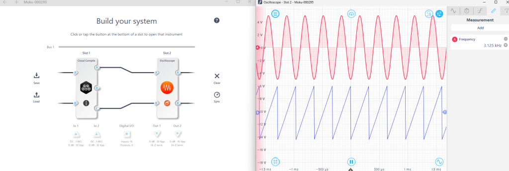
Figure 14: The Moku Oscilloscope inputs are connected to OutputA and OutputC of Moku Cloud Compile. The blue trace represents the most significant 16 bits of the phase counter output.
6. FIR_Filter_7coef
The FIR_Filter_7coef IP core operates at the full clock rate with fixed coefficients, offering a resource-efficient solution for users who need to integrate a low-pass filter into their Moku Cloud Compile designs without requiring additional instruments in the Multi-Instrument Mode setup. The filter coefficients are listed in Table 8, and the port definitions are provided in Table 9.
For applications requiring adjustable coefficients, users can either use the Moku FIR Filter Builder or recompile a custom FIR filter IP core by following the guidelines in the Customized IP cores section in this paper.
Table 8: Coefficients used in FIR_Filter_7coef.
Table 9: Port definitions of FIR_Filter_7coef.
| Name | Direction | Description |
| aclk | Input | Rising-edge clock. |
| s_axis_data_tvalid | Input | tvalid for input data channel. Asserted by external block to indicate data is available for transfer. |
| s_axis_data_tready | Output | tready for input data channel. Asserted by core to indicate core is ready to accept data. |
| s_axis_data_tdata [15:0] | Input | tdata for input data channel. Conveys the data stream to be filtered. See tdata Structure for internal structure |
| m_axis_data_tvalid | Output | tvalid for output data channel. Asserted by core to indicate data is available for transfer. |
| m_axis_data_tdata [23:0] | Output | tdata for the output data channel. This is the filtered data stream. See tdata Structure for internal structure. |
The VHDL instantiation of the FIR_Filter_7coef IP core is provided in Code 6. In this example, handshake signals are omitted, as the filter is designed to process continuous input data and produce a continuous output stream. To ensure proper output scaling, the most significant 16 bits of the filter output are routed to OutputA.
This application note examines the implementation of a dual boxcar averager, outlining its core structure, which comprises four single boxcar averagers group
Code 6: VHDL example of instantiating the FIR_Filter_7coef IP core.
LIBRARY ieee;

ARCHITECTURE Behavioural OF CustomWrapper IS

	SIGNAL FIR_out_temp : STD_LOGIC_VECTOR(23 DOWNTO 0);

BEGIN

	FIR_Filter : FIR_Filter_7coef
	PORT MAP(
		aclk => clk,
		-- input data is always valid
		s_axis_data_tvalid => '1',
		-- FIR filter ready to accept data
		s_axis_data_tready => OPEN,
		s_axis_data_tdata => InputA,

		-- FIR filtered data is available to be transferred
		m_axis_data_tvalid => OPEN,
		m_axis_data_tdata => FIR_out_temp
	);

	OutputA <= signed(FIR_out_temp(23 DOWNTO 8));

END ARCHITECTURE;
The FIR_Filter_7coef Multi-Instrument Mode test setup is shown in Figure 15. The filter response, as measured by the Moku Frequency Response Analyzer, is presented in Figure 16. A comparison between the simulated response and the measured response is shown in Figure 17. 
Figure 15: Multi-Instrument Mode configuration of the FIR_Filter_7coef IP core.
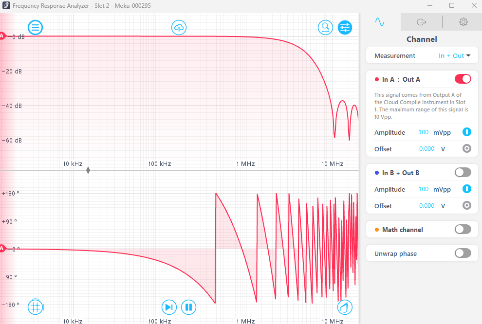
Figure 16: Frequency response obtained using the Moku Frequency Response Analyzer.
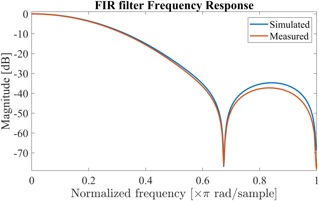
Figure 17: A comparison between the simulated response based on the given FIR coefficients and the measured frequency response.
7. FFT_1024
The Fast Fourier Transform (FFT) IP core implements the Cooley-Tukey algorithm, an efficient technique for computing the Discrete Fourier Transform (DFT). It is well-suited for applications such as large-scale filtering, cross-correlation, and coarse frequency analysis. Table 10 provides the input and output definitions for FFT_1024. This section presents an example implementation of the FFT core.
Table 10: Port definitions of the FFT_1024 IP core.
| Name | Direction | Description |
| aclk | Input | Rising-edge clock. |
| aresetn | Input | Active-Low synchronous clear (optional, always take priority over aclken). A minimum aresetn active pulse of two cycles is required. |
| s_axis_config_tdata[7:0] | Input | tdata for the Configuration channel. Carries the configuration information: CP_LEN, FWD/INV, NFFT and SCALE_SCH.
Only the least significant bit (0th bit) is used to control the FWD/INV (forward or inverse FFT). Other bits are empty. |
| s_axis_config_tvalid | Input | tvalid for the Configuration channel. Asserted by the external block to signal that it is able to provide data. |
| s_axis_config_tready | Output | tready for the Configuration channel. Asserted by the core to signal that it is ready to accept configuration data. |
| s_axis_data_tdata[31:0] | Input | tdata for the Data Input channel. Carries the unprocessed sample data: real part is [15:0] and imaginary part is [31:16]. |
| s_axis_data_tvalid | Input | tvalid for the Data Input channel. Used by the external block to signal that it is able to provide data. It can be set as constant high. |
| s_axis_data_tready | Output | tready for the Data Input channel. Used by the core to signal that it is ready to accept data. |
| s_axis_data_tlast | Input | tlast for the Data Input channel. Asserted by the external block on the last sample of the frame. This is not used by the core except to generate the events event_tlast_unexpected and event_tlast_missing events |
| m_axis_data_tdata[63:0] | Output | tdata for the Data Output channel. Carries the processed sample data real part is [58:32] and imaginary part is [26:0]. Signals are both signed 27-bit with 15 fractional bits. |
| m_axis_data_tuser[15:0] | Output | tuser for the Data Output channel. Carries the index of per-sample information. |
| m_axis_data_tvalid | Output | tvalid for the Data Output channel. Asserted by the core to signal that it is able to provide sample data. |
| m_axis_data_tready | Input | tready for the Data Output channel. Asserted by the external slave to signal that it is ready to accept data. |
| m_axis_data_tlast | Output | tlast for the Data Output channel. Asserted by the core on the last sample of the frame. |
| event_frame_started | Output | Asserted when the core starts to process a new frame. |
| event_tlast_unexpected | Output | Asserted when the core sees s_axis_data_tlast High on a data sample that is not the last one in a frame. |
| event_tlast_missing | Output | Asserted when s_axis_data_tlast is Low on the last data sample of a frame. |
| event_status_channel_halt | Output | Asserted when the core tries to write data to the Status channel and it is unable to do so. |
| event_data_in_channel_halt | Output | Asserted when the core requests data from the Data Input channel and none is available. |
| event_data_out_channel_halt | Output | Asserted when the core tries to write data to the Data Output channel and it is unable to do so. |
The VHDL instantiation of the FFT_1024 IP core is provided in Code 7. Since the input signal is purely real, only the least significant 16 bits of s_axis_data_tdata are connected to InputA, and the most significant 16 bits of both the real and imaginary components of the FFT output are connected to the inputs of the Cordic_Translate_16 module, which computes the corresponding amplitude and phase.
In this example, the FFT is configured as a forward Fourier transform through hardcoded settings by setting LSB of s_axis_config_tdata to high. Event signals are deliberately left unconnected, as they are not utilized in this example. The end of each FFT frame is indicated by the m_axis_data_tlast signal, upon which the FFT core is reset to prepare for the next processing cycle.
To account for the 20-cycle processing latency of the Cordic_Translate_16, the FFT output index (m_axis_data_tuser) is delayed accordingly. The resulting amplitude, phase, and frequency bin index are routed to OutputA, OutputB, and OutputC, respectively.
Code 7: VHDL example demonstrating the instantiation of the FFT_1024 IP core along with the Cordic_Translate_16 module, used to convert the FFT output into corresponding amplitude and phase values.
LIBRARY IEEE;
USE IEEE.STD_LOGIC_1164.ALL;
USE IEEE.NUMERIC_STD.ALL;

ARCHITECTURE Behavioural OF CustomWrapper IS

	TYPE array_tuser IS ARRAY (0 TO 19) OF signed(15 DOWNTO 0);

	SIGNAL aresetn, aresetn_dly : STD_LOGIC;

	SIGNAL s_axis_data_tdata : STD_LOGIC_VECTOR(31 DOWNTO 0);
	SIGNAL s_axis_data_tready : STD_LOGIC;

	SIGNAL m_axis_data_tlast : STD_LOGIC;
	SIGNAL m_axis_data_tvalid, m_axis_data_tvalid_dly : STD_LOGIC;
	SIGNAL m_axis_data_tuser : signed(15 DOWNTO 0);
	SIGNAL m_axis_data_tuser_dly : array_tuser;

	SIGNAL m_axis_dout_tvalid : STD_LOGIC;
	SIGNAL tdata_temp : signed(31 DOWNTO 0);

	SIGNAL im, real : STD_LOGIC_VECTOR(26 DOWNTO 0);

	SIGNAL fftdata_temp : STD_LOGIC_VECTOR(63 DOWNTO 0);

BEGIN

	FFT_DUT : FFT_1024
	PORT MAP(
		aclk => clk,
		aresetn => (NOT reset) AND aresetn AND aresetn_dly,
		-- Forward FFT with the LSB configured as 1
		s_axis_config_tdata => x"01",
		-- Config data is always valid
		s_axis_config_tvalid => '1',
		-- Leave config ready signal open
		-- config data is constant
		s_axis_config_tready => OPEN,
		-- Input only has real values
		s_axis_data_tdata => s_axis_data_tdata,
		-- Input data is always valid
		s_axis_data_tvalid => '1',
		-- Data ready logic
		s_axis_data_tready => s_axis_data_tready,
		-- Continuous data stream
		-- don't have last sample
		s_axis_data_tlast => '0',

		-- Transformed data
		m_axis_data_tdata => fftdata_temp,
		-- FFT frequency index
		m_axis_data_tuser => m_axis_data_tuser,
		-- output is valid
		m_axis_data_tvalid => m_axis_data_tvalid,
		-- Slave device is always ready to accept output
		m_axis_data_tready => '1',
		-- last sample of the frame
		m_axis_data_tlast => m_axis_data_tlast,

		-- don't care events
		event_frame_started => OPEN,
		event_tlast_unexpected => OPEN,
		event_tlast_missing => OPEN,
		event_status_channel_halt => OPEN,
		event_data_in_channel_halt => OPEN,
		event_data_out_channel_halt => OPEN
	);

	-- only output data when data is valid
	PROCESS (clk)
	BEGIN
		IF rising_edge(clk) THEN

			IF s_axis_data_tready THEN
				s_axis_data_tdata <= x"0000" & STD_LOGIC_VECTOR(InputA);
			END IF;

			IF m_axis_data_tvalid THEN
				im <= fftdata_temp(58 DOWNTO 32);
				real <= fftdata_temp(26 DOWNTO 0);
			END IF;
			m_axis_data_tuser_dly <= m_axis_data_tuser & m_axis_data_tuser_dly(0 TO 18);
		END IF;
	END PROCESS;
	-- reset process
	-- reset fft when the tlast is high
	PROCESS (clk)
	BEGIN
		IF rising_edge(Clk) THEN

			aresetn_dly <= aresetn;
			IF m_axis_data_tlast THEN
				aresetn <= '0';
			ELSE
				aresetn <= '1'; END IF; END IF; END PROCESS; Cordic : Cordic_Translate_16 PORT MAP( aclk => clk,
		s_axis_cartesian_tvalid => m_axis_data_tvalid,
		s_axis_cartesian_tdata => STD_LOGIC_VECTOR(im(26 DOWNTO 11) & real(26 DOWNTO 11)),
		m_axis_dout_tvalid => m_axis_dout_tvalid,
		m_axis_dout_tdata => tdata_temp
	);
	PROCESS (clk)
	BEGIN
		IF rising_edge(clk) THEN

			IF m_axis_dout_tvalid THEN
				OutputA <= signed(tdata_temp(15 DOWNTO 0));
				OutputB <= signed(tdata_temp(31 DOWNTO 16));
				OutputC <= signed(m_axis_data_tuser_dly(19));
			END IF;

		END IF;
	END PROCESS;

END ARCHITECTURE;
The Multi-Instrument Mode test configurations and corresponding output signals are shown in Figure 18 and Figure 19. Figure 18 illustrates the measurement setup for the amplitude output from the FFT_1024 and Cordic_Translate_16 IP cores, while Figure 19 shows the configuration for capturing the phase output.
In Figure 18, two peaks are visible in the amplitude spectrum, one in the positive frequency range and the other in the negative. The index associated with the positive frequency peak corresponds to a timestamp relative to the beginning of the index ramp. Given that the Moku:Go clock operates at 31.25 MHz and the total time span of the index ramp is 32.684 microseconds, the estimated frequency is calculated as:
![]()
\(text{Frequency} = frac{text{10.531 } mu text{s}}{text{32.684 } mu text{s}} times text{31.25 MHz} = text{10.0689 MHz}\)
It is important to note that the 1024-point FFT results in a resolution bandwidth of approximately 0.03 MHz. Therefore, this implementation is suitable for coarse frequency estimation only. For more precise analysis, it is recommended to use the Moku Phasemeter.
Figure 19 displays the phase output in red. The phase appears unstable due to the variability of the FFT analysis window across acquisition cycles. This example serves as a functional demonstration but does not constitute a complete spectrum analyzer, as it lacks essential components such as a windowing function and a superheterodyne block.
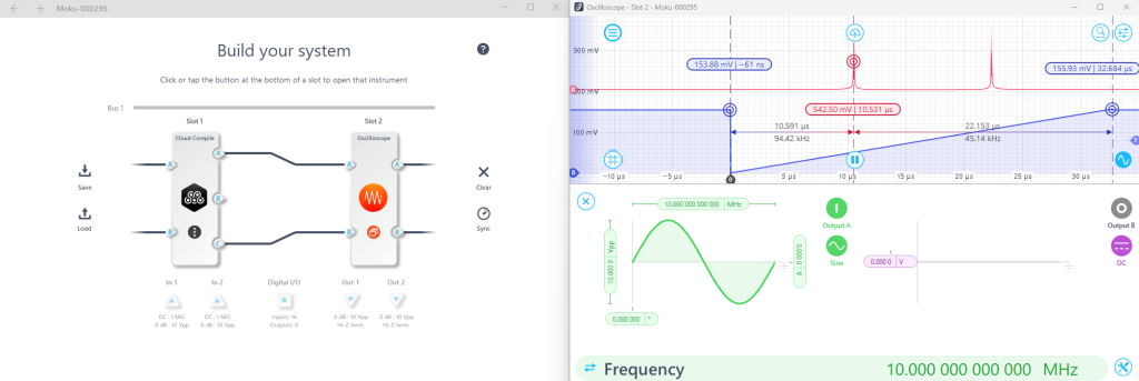
Figure 18: Multi-Instrument Mode test configuration and amplitude output results for the FFT_1024 IP core. A 10 MHz sine wave is applied to InputA of the Moku Cloud Compile and processed by the FFT_1024 module. The resulting amplitude spectrum, displayed on Channel A (red), reveals two peaks corresponding to the positive and negative frequency components of the input signal.
Figure 19: Multi-Instrument Mode test configuration and phase response of the FFT_1024 IP core. The observed phase response appears unstable due to the random time offset of the FFT analysis window relative to the input signal.
8. FFT_65536
FFT_65536 is a variant of FFT_1024, generated using the same IP core compiler but configured with a larger number of FFT points. Although both cores share the same foundation, FFT_65536 has distinct configuration parameters and output data formats to accommodate the increased point count. Detailed port specifications and updated signal connections are provided in Table 11, with changes highlighted.
Due to hardware resource limitations, the FFT_65536 IP core is not supported on Moku:Go or Moku:Lab and must be deployed on Moku:Pro.
Table 11: Ports definitions of FFT_65536 IP core. The parameters different than the FFT_1024 are bolded.
| Name | Direction | Description |
| aclk | Input | Rising-edge clock. |
| aresetn | Input | Active-Low synchronous clear (optional, always take priority over aclken). A minimum aresetn active pulse of two cycles is required. |
| s_axis_config_tdata[39:0] | Input | tdata for the Configuration channel. The 0th bit controls the forward or inverse FFT. And [32:1] is the scale of the output. Other bits are empty. |
| s_axis_config_tvalid | Input | tvalid for the Configuration channel. |
| s_axis_config_tready | Output | tready for the Configuration channel. |
| s_axis_data_tdata[31:0] | Input | tdata for the Data Input channel. Carries the unprocessed sample data: real [15:0] and imaginary [31:16]. |
| s_axis_data_tvalid | Input | tvalid for the Data Input channel. Set to constant high. |
| s_axis_data_tready | Output | tready for the Data Input channel. Used by the core to signal that it is ready to accept data. |
| s_axis_data_tlast | Input | tlast for the Data Input channel. Asserted by the external master on the last sample of the frame. |
| m_axis_data_tdata[31:0] | Output | tdata for the Data Output channel. Carries the processed sample data real [15:0] and imaginary [31:16]. The signal format is signed 16-bit with 15 fractional bits. |
| m_axis_data_tuser[15:0] | Output | tuser for the Data Output channel. Carries the index of per-sample information. |
| m_axis_data_tvalid | Output | tvalid for the Data Output channel. Asserted by the core to signal that it is able to provide sample data. |
| m_axis_data_tready | Input | tready for the Data Output channel. Asserted by the external block to signal that it is ready to accept data. |
| m_axis_data_tlast | Output | tlast for the Data Output channel. Asserted by the core on the last sample of the frame. |
| event_frame_started | Output | Asserted when the core starts to process a new frame. |
| event_tlast_unexpected | Output | Asserted when the core sees s_axis_data_tlast High on a data sample that is not the last one in a frame. |
| event_tlast_missing | Output | Asserted when s_axis_data_tlast is Low on the last data sample of a frame. |
| event_status_channel_halt | Output | Asserted when the core tries to write data to the Status channel and it is unable to do so. |
| event_data_in_channel_halt | Output | Asserted when the core requests data from the Data Input channel and none is available. |
| event_data_out_channel_halt | Output | Asserted when the core tries to write data to the Data Output channel and it is unable to do so. |
The VHDL example for instantiating FFT_65536 and one Cordic_Translate_16 is shown in Code 8. The Moku Cloud Compile outputs include the amplitude and phase spectra of InputA, along with the frequency index. Additionally, Control0 is used to set the scale parameter, and the LSB of Control1 determines the FFT direction.
Code 8: VHDL example demonstrating the instantiation of one FFT_65536 and one Cordic_Translate_16 module.
LIBRARY ieee;

ARCHITECTURE Behavioural OF CustomWrapper IS

	TYPE array_tuser IS ARRAY (0 TO 19) OF signed(15 DOWNTO 0);

	SIGNAL aresetn, aresetn_dly : STD_LOGIC;

	SIGNAL s_axis_data_tdata : STD_LOGIC_VECTOR(31 DOWNTO 0);
	SIGNAL s_axis_data_tready : STD_LOGIC;

	SIGNAL m_axis_data_tlast : STD_LOGIC;
	SIGNAL m_axis_data_tvalid, m_axis_data_tvalid_dly : STD_LOGIC;
	SIGNAL count_out, m_axis_data_tuser : signed(15 DOWNTO 0);
	SIGNAL m_axis_data_tuser_dly : array_tuser;

	SIGNAL fftdata_temp : signed(31 DOWNTO 0);
	SIGNAL real, im : signed(15 DOWNTO 0);

	SIGNAL m_axis_dout_tvalid : STD_LOGIC;
	SIGNAL tdata_temp : signed(31 DOWNTO 0);

BEGIN

	FFT_DUT : FFT_65536
	PORT MAP(
		aclk => clk,
		-- aresetn => (not Reset) and FFT_reset and FFT_reset_dly,
		aresetn => (NOT reset) AND aresetn AND aresetn_dly,
		-- Control FFT direction with LSB of Control1
		-- and scale of the FFT output with Control0
		s_axis_config_tdata => "0000000" & Control0(31 DOWNTO 0) & Control1(0),
		-- Config data is always valid
		s_axis_config_tvalid => '1',
		-- Leave config ready signal open
		-- config data is constant
		s_axis_config_tready => OPEN,
		-- Input only has real values
		s_axis_data_tdata => s_axis_data_tdata,
		-- Input data is always valid
		s_axis_data_tvalid => '1',
		-- Data ready logic
		s_axis_data_tready => s_axis_data_tready,
		-- Continuous data stream
		-- don't have last sample
		s_axis_data_tlast => '0',

		-- Transformed data
		m_axis_data_tdata => fftdata_temp,
		-- FFT frequency index
		m_axis_data_tuser => m_axis_data_tuser,
		-- output is valid
		m_axis_data_tvalid => m_axis_data_tvalid,
		-- Slave device is always ready to accept output
		m_axis_data_tready => '1',
		-- last sample of the frame
		m_axis_data_tlast => m_axis_data_tlast,

		-- don't care events
		event_frame_started => OPEN,
		event_tlast_unexpected => OPEN,
		event_tlast_missing => OPEN,
		event_status_channel_halt => OPEN,
		event_data_in_channel_halt => OPEN,
		event_data_out_channel_halt => OPEN
	);

	-- only output data when data is valid
	PROCESS (clk)
	BEGIN
		IF rising_edge(clk) THEN

			IF s_axis_data_tready THEN
				s_axis_data_tdata <= x"0000" & STD_LOGIC_VECTOR(InputA);
			END IF;

			IF m_axis_data_tvalid THEN
				-- real part
				real <= fftdata_temp(15 DOWNTO 0);
				-- imaginary part
				im <= fftdata_temp(31 DOWNTO 16);
			END IF;
			-- delay 20 clk cycles
			m_axis_data_tuser_dly <= m_axis_data_tuser & m_axis_data_tuser_dly(0 TO 18);
		END IF;
	END PROCESS;
	-- reset process
	-- reset fft when the tlast is high
	PROCESS (clk)
	BEGIN
		IF rising_edge(Clk) THEN

			aresetn_dly <= aresetn;
			IF m_axis_data_tlast THEN
				aresetn <= '0';
			ELSE
				aresetn <= '1'; END IF; END IF; END PROCESS; Cordic : Cordic_Translate_16 PORT MAP( aclk => clk,
		s_axis_cartesian_tvalid => m_axis_data_tvalid,
		s_axis_cartesian_tdata => STD_LOGIC_VECTOR(im & real),
		m_axis_dout_tvalid => m_axis_dout_tvalid,
		m_axis_dout_tdata => tdata_temp
	);
	PROCESS (clk)
	BEGIN
		IF rising_edge(clk) THEN

			IF m_axis_dout_tvalid THEN
				OutputA <= signed(tdata_temp(15 DOWNTO 0));
				OutputB <= signed(tdata_temp(31 DOWNTO 16));
				OutputC <= signed(m_axis_data_tuser_dly(19));
			END IF;

		END IF;
	END PROCESS;

END ARCHITECTURE;
The Moku:Pro Multi-Instrument Mode test configurations are shown in Figure 20. The signal under test is generated by the Moku Oscilloscope’s built-in waveform generator and routed back to the Moku Cloud Compile input via the internal digital signal bus. Moku Cloud Compile produces three outputs: OutputA and OutputB represent the converted amplitude and phase, while OutputC corresponds to the frequency index. These outputs are connected to the inputs of the Oscilloscope for monitoring.
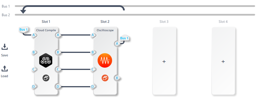
Figure 20: Moku:Pro FFT_65536 testing Multi-Instrument Mode configurations.
The output amplitude and frequency index of FFT_65536 are shown in Figure 21. Control0 is fine-tuned to prevent signal overflow, and Control1 is set to 1 to perform a forward FFT. It is worth noting that the frequency index appears to flip signs due to the use of a signed 16-bit representation for the 65,536-point FFT, which results in an overflow. However, this overflow is harmless, as it effectively distinguishes between negative and positive frequencies. The amplitude channel shows a peak near the 80 MHz frequency index, which corresponds to the 80 MHz input signal from Moku Cloud Compile, given the Moku:Pro Moku Cloud Compile clock rate of 312.5 MHz.
![]()
\(text{Frequency} = frac{53.86 mu text{s}}{104.95 mu text{s}} times frac{312.5 text{MHz}}{2} = 80.19 text{MHz}\)
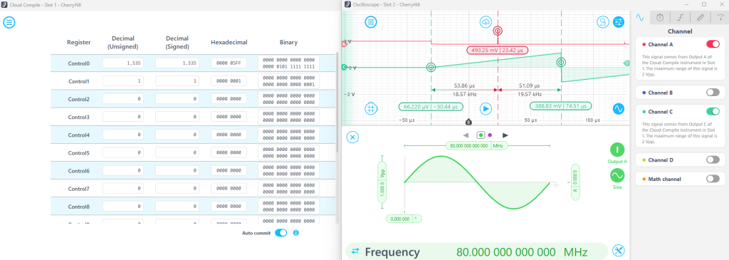
Figure 21: Test results of the instantiated FFT_65536 and its corresponding amplitude spectrum output.
Customized IP cores
Moku Cloud Compile also allows users to upload custom .xci files that define the configuration of IP cores generated in Vivado. Moku Cloud Compile is capable of parsing these .xci files, loading the corresponding IP cores on the backend, and enabling their instantiation within user designs.
It is important to note that the .xci files must be generated using Vivado version 2022.2 to ensure compatibility with the Moku Cloud Compile backend. All IP cores supported by Vivado 2022.2 are likewise supported by Moku Cloud Compile. Vivado 2022.2 is available for download from the official AMD website. The following section presents an example to illustrate this process.
1. Create Vivado project:
Selecting the correct hardware platform is essential during the project creation process. The target FPGA device must be specified as part of the setup process. Table 12 lists the FPGA platform models for three supported hardware platforms, and an example configuration is illustrated in Figure 22.
Table 12: The FPGA model numbers of the Moku platforms.
| Platform | FPGA model |
| Moku:Go | xc7z020clg400-1 |
| Moku:Lab | xc7z020clg484-3 |
| Moku:Pro | xczu9egffvc900-2 |
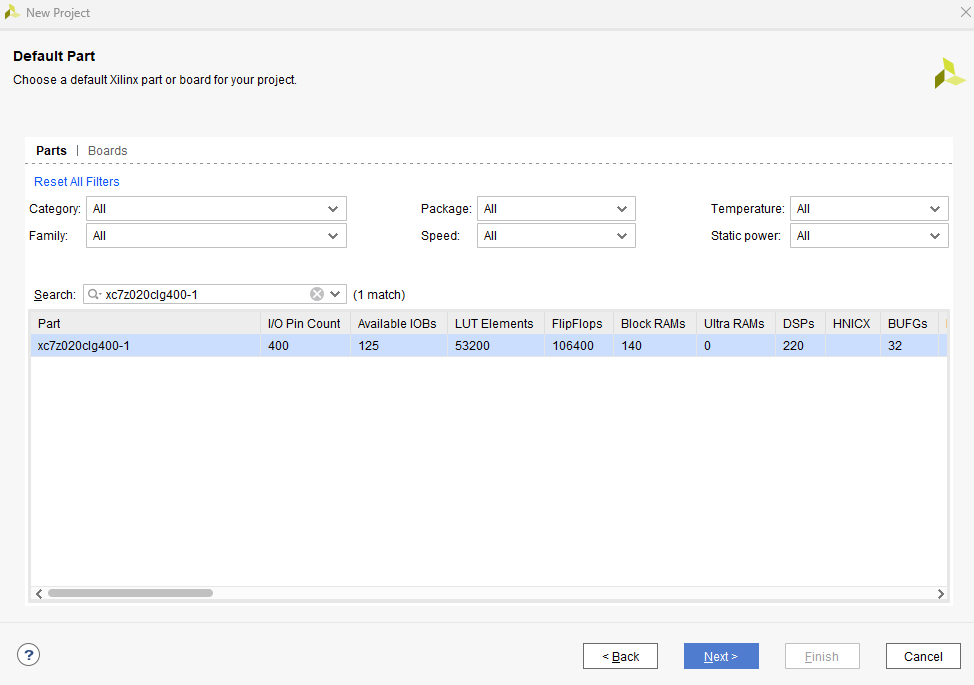
Figure 22: The project must be created in Vivado with the appropriate FPGA platform settings. In this example, the Moku:Go platform is selected as the target device.
2. Build an IP core and locate the .xci file
A custom IP core can be compiled by following the steps illustrated in Figure 23. First, select IP Catalog from the Project Manager panel on the left (Step 1). Then, choose the desired IP core from the list in the right panel (Step 2). During configuration, the clock frequency may be required; platform-specific clock rates are provided in Table 13. Once the IP core is configured, it will appear in the Sources window (Step 3). The location of the generated .xci file can be found in the Source File Properties panel (Step 4).
Table 13: Clock rates of Moku Cloud Compile across different hardware platforms.
| Platform | Moku Cloud Compile clock rate (MHz) |
| Moku:Go | 31.25 |
| Moku:Lab | 125 |
| Moku:Pro |
312.5 |

Figure 23: The process of configuring the IP core.
3. Upload .xci file to Moku Cloud Compile and change OUTPUTDIR
Once the IP core has been compiled, the .xci file should be uploaded to the Moku Cloud Compile web interface. To ensure successful recompilation on the Moku Cloud Compile backend, the OUTPUTDIR parameter must be set to “../output“. An example of this process is illustrated in Figure 24.
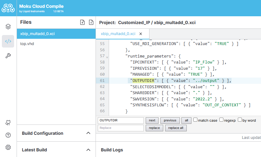
Figure 24: Upload the .xci file to Moku Cloud Compile and set the OUTPUTDIR to “../output“ to ensure proper compilation.
4. Instantiate the IP core in Moku Cloud Compile and build the design
To instantiate a custom IP core in Moku Cloud Compile, it is essential to understand the port configurations and signal connections. Figure 25 illustrates the process of locating the instantiation template. Begin by selecting IP Sources, then locate the .vho and .veo files, which provide example instantiations. The .vho file is intended for VHDL, while the .veo file is used for Verilog.
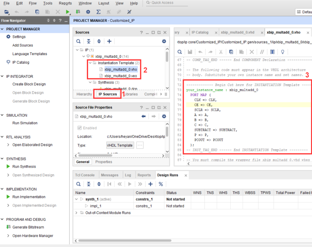
Figure 25: Locating the IP core instantiating templates.
Next, the process of instantiating the custom IP core using the templates is shown in Figure 26. This completes the setup, after which the custom IP core can be compiled within Moku Cloud Compile and the bitstreams are generated.
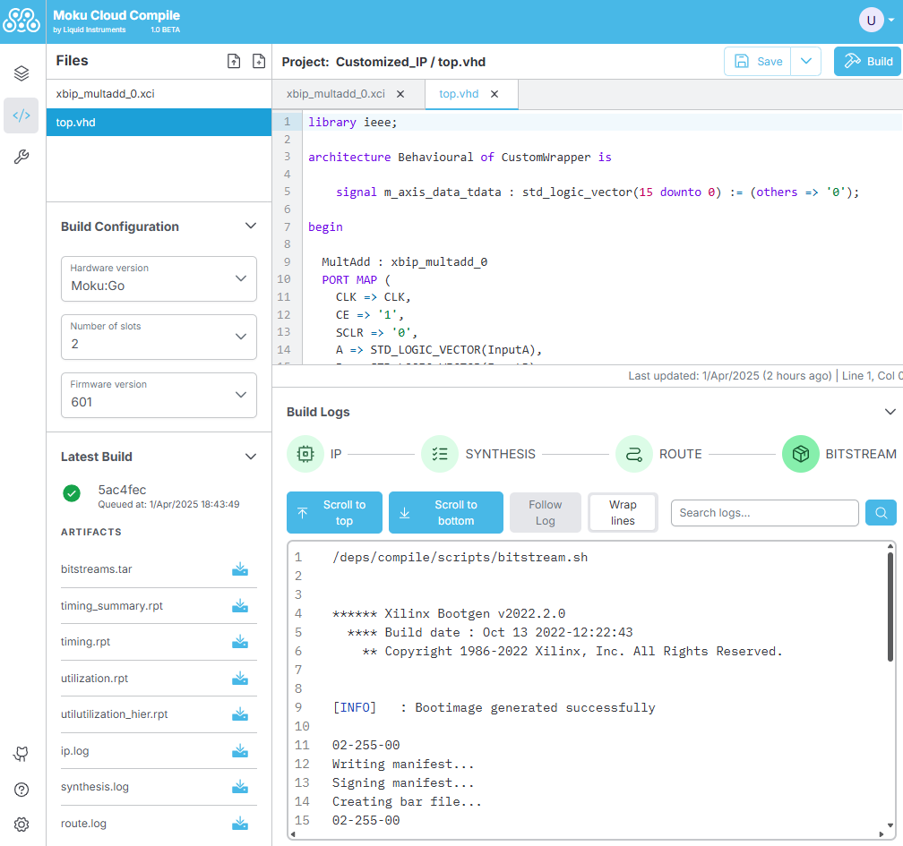
Figure 26: Instantiate the IP core within Moku Cloud Compile and connect its signals to the corresponding ports of the CustomWrapper module.
Verilog support
Verilog, like VHDL, is a hardware description language, but it is generally more compact and closely aligned with hardware modeling. In contrast to VHDL, where users typically define only the behavior architecture of the CustomWrapper entity, Verilog requires both the declaration and structural definition of the entire CustomWrapper module. This includes explicitly specifying the CustomWrapper ports and internal logic.
This section provides an example of instantiating the AddSubtract_16 IP core using Verilog, as shown in Code 9. It is important to note that Verilog is case-sensitive. Therefore, correct capitalization and consistent naming are essential to avoid synthesis or behavioral errors.
Code 9: Example Verilog implementation demonstrating support for the AddSubtract_16 IP core.
module CustomWrapper (
    input wire Clk,
    input wire Reset,
    input wire [31:0] Sync,

    // 4 input ports
    input wire signed [15:0] InputA,
    input wire signed [15:0] InputB,
    input wire signed [15:0] InputC,
    input wire signed [15:0] InputD,

    // external trigger input port
    input wire ExtTrig,

    // 4 output ports
    output wire signed [15:0] OutputA,
    output wire signed [15:0] OutputB,
    output wire signed [15:0] OutputC,
    output wire signed [15:0] OutputD,

    // enable/disable interpolation
    output wire OutputInterpA,
    output wire OutputInterpB,
    output wire OutputInterpC,
    output wire OutputInterpD,

    // 16 control registers
    input wire [31:0] Control0,
    input wire [31:0] Control1,
    input wire [31:0] Control2,
    input wire [31:0] Control3,
    input wire [31:0] Control4,
    input wire [31:0] Control5,
    input wire [31:0] Control6,
    input wire [31:0] Control7,
    input wire [31:0] Control8,
    input wire [31:0] Control9,
    input wire [31:0] Control10,
    input wire [31:0] Control11,
    input wire [31:0] Control12,
    input wire [31:0] Control13,
    input wire [31:0] Control14,
    input wire [31:0] Control15
);

AddSubtract_16 AddSubtract_DUT (
  .A(InputA),      // input wire [15 : 0] A
  .B(InputB),      // input wire [15 : 0] B
  .CLK(Clk),  // input wire CLK
  .ADD(Control0[0]),  // input wire ADD
  .CE(1'b1),    // input wire CE
  .S(OutputA)      // output wire [15 : 0] S
);

endmodule
After uploading the example Verilog code to Moku Cloud Compile, the AddSubtract_16 module can be compiled successfully, and the corresponding bitstream is generated, as illustrated in Figure 27. 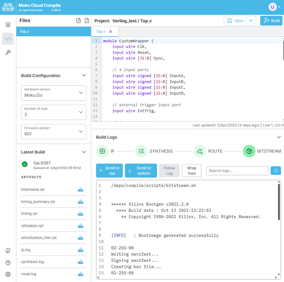
Figure 27: Moku Cloud Compile interface for compiling the AddSubtract_16 module and generating bitstreams from Verilog code.
Summary
Moku Cloud Compile offers eight precompiled IP cores for signal processing tasks such as arithmetic operations, filtering, waveform generation, and spectral analysis. Each core is described above with detailed port definitions, example VHDL implementations, and test configurations using Multi-Instrument Mode on Moku hardware platforms.
In addition to built-in cores, users can upload custom IP cores by importing .xci files generated in Vivado 2022.2. Moku Cloud Compile also offers both Verilog and VHDL support. Together, these features enhance Moku Cloud Compile’s capabilities, making it a powerful and flexible platform for rapid development and deployment of FPGA-based digital signal processing solutions.